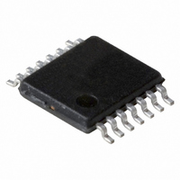
74HC73DB,112 NXP Semiconductors, 74HC73DB,112 Datasheet - Page 7

74HC73DB,112
Manufacturer Part Number
74HC73DB,112
Description
IC DUAL JK FF NEG-EDGE 14-SSOP
Manufacturer
NXP Semiconductors
Series
74HCr
Type
JK Typer
Datasheet
1.74HC73N652.pdf
(16 pages)
Specifications of 74HC73DB,112
Output Type
Differential
Package / Case
14-SSOP
Function
Reset
Number Of Elements
2
Number Of Bits Per Element
1
Frequency - Clock
77MHz
Delay Time - Propagation
15ns
Trigger Type
Negative Edge
Current - Output High, Low
5.2mA, 5.2mA
Voltage - Supply
2 V ~ 6 V
Operating Temperature
-40°C ~ 125°C
Mounting Type
Surface Mount
Number Of Circuits
2
Logic Family
HC
Logic Type
J-K Negative Edge Triggered Flip Flop
Polarity
Inverting/Non-Inverting
Input Type
Single-Ended
Propagation Delay Time
16 ns at 5 V
High Level Output Current
- 5.2 mA
Low Level Output Current
5.2 mA
Supply Voltage (max)
6 V
Maximum Operating Temperature
+ 125 C
Mounting Style
SMD/SMT
Minimum Operating Temperature
- 40 C
Supply Voltage (min)
2 V
Lead Free Status / RoHS Status
Lead free / RoHS Compliant
Lead Free Status / RoHS Status
Lead free / RoHS Compliant, Lead free / RoHS Compliant
Other names
568-2736-5
935190270112
935190270112
Available stocks
Company
Part Number
Manufacturer
Quantity
Price
Company:
Part Number:
74HC73DB,112
Manufacturer:
IDT
Quantity:
123
NXP Semiconductors
Table 7.
GND (ground = 0 V); C
[1]
[2]
[3]
74HC73_4
Product data sheet
Symbol Parameter
t
f
C
h
max
PD
t
t
C
P
f
f
C
V
N = number of inputs switching;
pd
t
i
o
D
CC
PD
= input frequency in MHz;
L
(C
is the same as t
= output frequency in MHz;
is the same as t
= output load capacitance in pF;
= C
L
is used to determine the dynamic power dissipation (P
= supply voltage in V;
PD
hold time
maximum
frequency
power
dissipation
capacitance
V
Dynamic characteristics
CC
2
V
CC
f
o
2
) = sum of outputs.
THL
PHL
f
i
L
, t
, t
= 50 pF unless otherwise specified; for test circuit, see
TLH
N + (C
PLH
Conditions
nJ, nK to nCP; see
nCP input; see
per flip-flop;
V
.
I
V
V
V
V
V
V
V
.
= GND to V
CC
CC
CC
CC
CC
CC
CC
L
= 2.0 V
= 4.5 V
= 6.0 V
= 2.0 V
= 4.5 V
= 6.0 V
= 5.0 V; C
V
CC
…continued
2
CC
f
Figure 6
o
) where:
L
= 15 pF
Figure 6
Rev. 04 — 19 March 2008
D
[3]
in W).
Min Typ Max
6.0
30
35
3
3
3
-
-
Dual JK flip-flop with reset; negative-edge trigger
25 C
23
70
83
77
30
8
3
2
-
-
-
-
-
-
-
-
Figure 8
40 C to +85 C
Min
4.8
24
28
3
3
3
-
Max
-
-
-
-
-
-
40 C to +125 C Unit
Min
4.0
20
24
3
3
3
-
© NXP B.V. 2008. All rights reserved.
74HC73
Max
-
-
-
-
-
-
-
7 of 16
ns
ns
ns
MHz
MHz
MHz
MHz
pF


