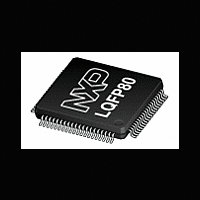
LPC1759FBD80 NXP Semiconductors, LPC1759FBD80 Datasheet - Page 12

LPC1759FBD80
Manufacturer Part Number
LPC1759FBD80
Description
The LPC1759 is a Cortex-M3 microcontroller for embedded applications featuring a high level of integration and low power consumption at frequencies of 120 MHz
Manufacturer
NXP Semiconductors
Datasheet
1.LPC1759FBD80.pdf
(74 pages)
Available stocks
Company
Part Number
Manufacturer
Quantity
Price
Company:
Part Number:
LPC1759FBD80
Manufacturer:
MICROCHIP
Quantity:
12 000
Part Number:
LPC1759FBD80
Manufacturer:
NXP/恩智浦
Quantity:
20 000
Company:
Part Number:
LPC1759FBD80,551
Manufacturer:
LT
Quantity:
375
Company:
Part Number:
LPC1759FBD80,551
Manufacturer:
NXP Semiconductors
Quantity:
10 000
Part Number:
LPC1759FBD80,551
Manufacturer:
NXP/恩智浦
Quantity:
20 000
NXP Semiconductors
Table 3.
[1]
[2]
[3]
[4]
[5]
[6]
[7]
[8]
[9]
[10] When the system oscillator is not used, connect XTAL1 and XTAL2 as follows: XTAL1 can be left floating or can be grounded (grounding
[11] When the RTC is not used, connect VBAT to V
LPC1759_58_56_54_52_51
Product data sheet
Symbol
V
V
V
V
VREFP
VREFN
VBAT
SSA
DD(3V3)
DD(REG)(3V3)
DDA
5 V tolerant pad providing digital I/O functions with TTL levels and hysteresis.
5 V tolerant pad providing digital I/O functions (with TTL levels and hysteresis) and analog input. When configured as a ADC input,
digital section of the pad is disabled and the pin is not 5 V tolerant.
5 V tolerant pad providing digital I/O with TTL levels and hysteresis and analog output function. When configured as the DAC output,
digital section of the pad is disabled.
Pad provides digital I/O and USB functions. It is designed in accordance with the USB specification, revision 2.0 (Full-speed and
Low-speed mode only). This pad is not 5 V tolerant.
5 V tolerant pad with 5 ns glitch filter providing digital I/O functions with TTL levels and hysteresis.
5 V tolerant pad with TTL levels and hysteresis. Internal pull-up and pull-down resistors disabled.
5 V tolerant pad with TTL levels and hysteresis and internal pull-up resistor.
5 V tolerant pad with 20 ns glitch filter providing digital I/O function with TTL levels and hysteresis.
Pad provides special analog functionality.
is preferred to reduce susceptibility to noise). XTAL2 should be left floating.
Pin description
Pin
9
21, 42,
56, 77
34, 67
8
10
12
16
[11]
…continued
Type
I
I
I
I
I
I
I
Description
analog ground: 0 V reference. This should nominally be the same voltage as V
but should be isolated to minimize noise and error.
3.3 V supply voltage: This is the power supply voltage for the I/O ports.
3.3 V voltage regulator supply voltage: This is the supply voltage for the on-chip
voltage regulator only.
analog 3.3 V pad supply voltage: This should be nominally the same voltage as
V
power the ADC and DAC. This pin should be tied to 3.3 V if the ADC and DAC are
not used.
ADC positive reference voltage: This should be nominally the same voltage as
V
as a reference for ADC and DAC. This pin should be tied to 3.3 V if the ADC and
DAC are not used.
ADC negative reference voltage: This should be nominally the same voltage as
V
a reference for ADC and DAC.
RTC pin power supply: 3.3 V on this pin supplies the power to the RTC
peripheral.
All information provided in this document is subject to legal disclaimers.
DD(3V3)
DDA
SS
but should be isolated to minimize noise and error. Level on this pin is used as
DD(REG)(3V3)
but should be isolated to minimize noise and error. Level on this pin is used
but should be isolated to minimize noise and error. This voltage is used to
Rev. 7 — 29 March 2011
and leave RTCX1 floating.
LPC1759/58/56/54/52/51
32-bit ARM Cortex-M3 microcontroller
© NXP B.V. 2011. All rights reserved.
12 of 74
SS
,


