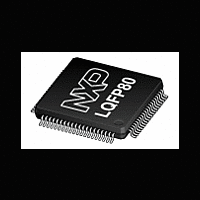
LPC1759FBD80 NXP Semiconductors, LPC1759FBD80 Datasheet - Page 10

LPC1759FBD80
Manufacturer Part Number
LPC1759FBD80
Description
The LPC1759 is a Cortex-M3 microcontroller for embedded applications featuring a high level of integration and low power consumption at frequencies of 120 MHz
Manufacturer
NXP Semiconductors
Datasheet
1.LPC1759FBD80.pdf
(74 pages)
Available stocks
Company
Part Number
Manufacturer
Quantity
Price
Company:
Part Number:
LPC1759FBD80
Manufacturer:
MICROCHIP
Quantity:
12 000
Part Number:
LPC1759FBD80
Manufacturer:
NXP/恩智浦
Quantity:
20 000
Company:
Part Number:
LPC1759FBD80,551
Manufacturer:
LT
Quantity:
375
Company:
Part Number:
LPC1759FBD80,551
Manufacturer:
NXP Semiconductors
Quantity:
10 000
Part Number:
LPC1759FBD80,551
Manufacturer:
NXP/恩智浦
Quantity:
20 000
NXP Semiconductors
Table 3.
LPC1759_58_56_54_52_51
Product data sheet
Symbol
P1[30]/V
AD0[4]
P1[31]/SCK1/
AD0[5]
P2[0] to P2[31]
P2[0]/PWM1[1]/
TXD1
P2[1]/PWM1[2]/
RXD1
P2[2]/PWM1[3]/
CTS1/
TRACEDATA[3]
P2[3]/PWM1[4]/
DCD1/
TRACEDATA[2]
P2[4]/PWM1[5]/
DSR1/
TRACEDATA[1]
P2[5]/PWM1[6]/
DTR1/
TRACEDATA[0]
P2[6]/PCAP1[0]/
RI1/TRACECLK
P2[7]/RD2/
RTS1
BUS
Pin description
/
Pin
18
17
60
59
58
55
54
53
52
51
[2]
[2]
[1]
[1]
[1]
[1]
[1]
[1]
[1]
[1]
…continued
Type
I/O
I
I
I/O
I/O
I
I/O
I/O
O
O
I/O
O
I
I/O
O
I
O
I/O
O
I
O
I/O
O
I
O
I/O
O
O
O
I/O
I
I
O
I/O
I
O
Description
P1[30] — General purpose digital input/output pin.
V
Note: This signal must be HIGH for USB reset to occur.
AD0[4] — A/D converter 0, input 4.
P1[31] — General purpose digital input/output pin.
SCK1 — Serial Clock for SSP1.
AD0[5] — A/D converter 0, input 5.
Port 2: Port 2 is a 32-bit I/O port with individual direction controls for each bit. The
operation of port 2 pins depends upon the pin function selected via the pin connect
block. Some port pins are not available on the LQFP80 package.
P2[0] — General purpose digital input/output pin.
PWM1[1] — Pulse Width Modulator 1, channel 1 output.
TXD1 — Transmitter output for UART1.
P2[1] — General purpose digital input/output pin.
PWM1[2] — Pulse Width Modulator 1, channel 2 output.
RXD1 — Receiver input for UART1.
P2[2] — General purpose digital input/output pin.
PWM1[3] — Pulse Width Modulator 1, channel 3 output.
CTS1 — Clear to Send input for UART1.
TRACEDATA[3] — Trace data, bit 3.
P2[3] — General purpose digital input/output pin.
PWM1[4] — Pulse Width Modulator 1, channel 4 output.
DCD1 — Data Carrier Detect input for UART1.
TRACEDATA[2] — Trace data, bit 2.
P2[4] — General purpose digital input/output pin.
PWM1[5] — Pulse Width Modulator 1, channel 5 output.
DSR1 — Data Set Ready input for UART1.
TRACEDATA[1] — Trace data, bit 1.
P2[5] — General purpose digital input/output pin.
PWM1[6] — Pulse Width Modulator 1, channel 6 output.
DTR1 — Data Terminal Ready output for UART1. Can also be configured to be an
RS-485/EIA-485 output enable signal.
TRACEDATA[0] — Trace data, bit 0.
P2[6] — General purpose digital input/output pin.
PCAP1[0] — Capture input for PWM1, channel 0.
RI1 — Ring Indicator input for UART1.
TRACECLK — Trace Clock.
P2[7] — General purpose digital input/output pin.
RD2 — CAN2 receiver input. (LPC1759/58/56 only).
RTS1 — Request to Send output for UART1. Can also be configured to be an
RS-485/EIA-485 output enable signal.
All information provided in this document is subject to legal disclaimers.
BUS
— Monitors the presence of USB bus power.
Rev. 7 — 29 March 2011
LPC1759/58/56/54/52/51
32-bit ARM Cortex-M3 microcontroller
© NXP B.V. 2011. All rights reserved.
10 of 74


