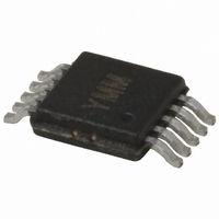
SY88813VKI TR Micrel Inc, SY88813VKI TR Datasheet - Page 5

SY88813VKI TR
Manufacturer Part Number
SY88813VKI TR
Description
IC AMP POST PECL 3.3V/5V 10-MSOP
Manufacturer
Micrel Inc
Type
Limiting Postamplifierr
Datasheet
1.SY88813VKG.pdf
(8 pages)
Specifications of SY88813VKI TR
Applications
Optical Networks
Mounting Type
Surface Mount
Package / Case
10-MSOP, Micro10™, 10-uMAX, 10-uSOP
Lead Free Status / RoHS Status
Contains lead / RoHS non-compliant
Other names
SY88813VKITR
SY88813VKITR
SY88813VKITR
Micrel, Inc.
from a single +3.3V or +5V power supply, over temperatures
from –40 C to +85 C. Signals with data rates up to 155Mbps
and as small as 5mV
the allowed input voltage swing. The SY88813V generates
a SD output. SD
detection.
Input Amplifier/Buffer
input stage. The high-sensitivity of the input amplifier allows
signals as small as 5mV
The input amplifier allows input signals as large as
1800mV
38dB differential voltage gain. Since it is a limiting amplifier,
the SY88813V outputs typically 1500mV
waveforms for input signals that are greater than 18mV
Applications requiring the SY88813V to operate with high-
gain should have the upstream TIA placed as close as
possible to the SY88813V’s input pins to ensure the best
performance of the device.
Output Buffer
50 lines. The output buffer requires appropriate termination
for proper operation. An external 50
for each output pin provides this. Figure 3 shows a simplified
schematic of the output stage and includes an appropriate
termination method.
M9999-072505
hbwhelp@micrel.com or (408) 955-1690
DETAILED DESCRIPTION
The SY88813V low power limiting post amplifier operates
Figure 2 shows a simplified schematic of the SY88813V's
The SY88813V’s PECL output buffer is designed to drive
PP
. Input signals are linearly amplified with a typically
LVL
sets the sensitivity of the input amplitude
PP
can be amplified. Figure 1 shows
PP
to be detected and amplified.
resistor to V
PP
voltage-limited
CC
–2V
PP
.
5
Signal-Detect
to the SY88813V's output buffer. SD is used to determine
that the input amplitude is large enough to be considered a
valid input. SD asserts high if the input amplitude rises
above the threshold set by SD
otherwise. /EN deasserts the true output signal without
removing the input signals. Typically 4.6dB SD hysteresis is
provided to prevent chattering.
Signal-Detect Level Set
the threshold of the input amplitude detection. Setting a
voltage on SD
If desired, a resistor divider between V
shown in Figure 4, also creates this threshold. The smaller
the voltage difference from SD
SD sensitivity. Hence, larger input amplitude is required to
assert SD. “Typical Operating Characteristics” shows the
relationship between the input amplitude detection sensitivity
and the SD
Hysteresis
hysteresis. By definition, a power ratio measured in dB is
10log(power ratio). Power is calculated as V
electrical signal. Hence the same ratio can be stated as
20log(voltage ratio). While in linear mode, the electrical
voltage input changes linearly with the optical power and
hence the ratios change linearly. Therefore, the optical
hysteresis in dB is half the electrical hysteresis in dB given
in the datasheet. The SY88813V provides typically 2.3dB
SD optical hysteresis. As the SY88813V is an electrical
device, this datasheet refers to hysteresis in electrical terms.
With 6dB SD hysteresis, a voltage factor of two is required
to assert or deassert SD.
The SY88813V generates a chatter-free PECL SD similar
A programmable signal-detect level set pin (SD
The SY88813V provides typically 4.6dB SD electrical
LVL
LVL
voltage.
between V
CC
and V
LVL
LVL
to V
REF
and deasserts low
CC
sets this threshold.
CC
, the smaller the
and V
2
IN
SY88813V
/R for an
LVL
REF
) sets
, as


