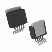
LME49600TS/NOPB National Semiconductor, LME49600TS/NOPB Datasheet - Page 4

LME49600TS/NOPB
Manufacturer Part Number
LME49600TS/NOPB
Description
IC AMP BUFFER AUD HI FI TO-263-5
Manufacturer
National Semiconductor
Type
Class ABr
Datasheet
1.LME49600TSNOPB.pdf
(20 pages)
Specifications of LME49600TS/NOPB
Output Type
1-Channel (Mono)
Max Output Power X Channels @ Load
500mW x 1 @ 32 Ohm
Voltage - Supply
±2.25 V ~ 18 V
Features
Short-Circuit and Thermal Protection
Mounting Type
Surface Mount
Package / Case
D²Pak, TO-263 (5 leads + tab)
Amplifier Class
AB
No. Of Channels
1
Supply Voltage Range
± 2.25V To ± 18V
Load Impedance
32ohm
Operating Temperature Range
-40°C To +85°C
Amplifier Case Style
TO-263
No. Of Pins
5
Rohs Compliant
Yes
Number Of Channels
1
Voltage Gain Db
0.09 dB
Input Voltage Range (max)
36 V
Input Voltage Range (min)
4.5 V
Input Offset Voltage
60 mV at +/- 15 V
Supply Current
14.5 mA
Maximum Operating Temperature
+ 85 C
Mounting Style
SMD/SMT
Maximum Dual Supply Voltage
+/- 18 V
Minimum Operating Temperature
- 40 C
Lead Free Status / RoHS Status
Lead free / RoHS Compliant
Other names
*LME49600TS/NOPB
LME49600TS
LME49600TS
www.national.com
V
I
I
I
Z
V
V
OUT
OUT-SC
B
Symbol
IN
OUT
OS
OS
Note 1: All voltages are measured with respect to ground, unless otherwise specified.
Note 2: Absolute Maximum Ratings indicate limits beyond which damage to the device may occur. Operating Ratings indicate conditions for which the device is
functional, but do not guarantee specific performance limits. Electrical Characteristics state DC and AC electrical specifications under particular test conditions
which guarantee specific performance limits. This assumes that the device is within the Operating Ratings. Specifications are not guaranteed for parameters
where no limit is given, however, the typical value is a good indication of device performance.
Note 3: The maximum power dissipation must be derated at elevated temperatures and is dictated by T
allowable power dissipation is P
application (shown in Figure 2) with V
copper surface heat sink area.
Note 4: Human body model, 100pF discharged through a 1.5kΩ resistor.
Note 5: Machine Model, 220pF – 240pF discharged through all pins.
Note 6: Typical specifications are specified at 25°C and represent the parametric norm.
Note 7: Tested limits are guaranteed to National's AOQL (Average Outgoing Quality Level).
Note 8: This is the distortion of the LME49600 operating in a closed loop configuration with an LME49710. When operating in an operational amplifier's feedback
loop, the amplifier’s open loop gain dominates, linearizing the system and determining the overall system distortion.
Note 9: The TSB package is non-isolated package. The package's metal back and any heat sink to which it is mounted are connected to the same potential as
the -V
/°C
EE
pin.
Voltage Output
Output Current
Short Circuit Output Current
Input Bias Current
Input Impedance
Offset Voltage
Offset Voltage vs Temperature
Parameter
DMAX
= (T
SUPPLY
JMAX
= 30V, R
–T
A
)/θ
JA
L
or the number given in Absolute Maximum Ratings, whichever is lower. For the LME49600, typical
= 32Ω, the total power dissipation is 1.9W. θ
Positive
I
I
I
Negative
I
I
I
BW pin: No Connect
BW pin: Connected to V
V
BW pin: No Connect
BW pin: Connected to V
R
BW pin: No Connect
BW pin: Connected to V
40°C
OUT
OUT
OUT
OUT
OUT
OUT
IN
L
= 100Ω
= 0V
= 10mA
= 100mA
= 150mA
= –10mA
= –100mA
= –150mA
≤
T
A
≤
Conditions
+125°C
4
EE
EE
EE
pin
pin
pin
JA
= 20°C/W for the TO–263 package mounted to 16in
JMAX
, θ
JA
V
V
V
V
V
V
(Note 6)
Typical
, and the ambient temperature T
CC
CC
CC
EE
EE
EE
±250
±490
±490
±100
±1.0
±3.0
±17
7.5
5.5
+1.5
+3.1
+3.5
–1.4
–2.0
–2.3
LME49600
V
V
V
V
V
V
(Note 7)
CC
CC
CC
EE
EE
EE
Limit
±550
±2.5
±5.0
±60
+1.6
+2.4
+3.2
–1.6
–2.1
–2.7
A
. The maximum
mA (max)
mA (max)
mV (max)
μA (max)
μA (max)
(Limits)
V (min)
V (min)
V (min)
V (min)
V (min)
V (min)
μV/°C
Units
MΩ
MΩ
mA
2
1oz


