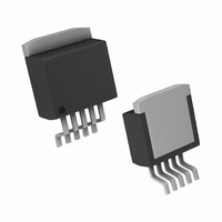
LME49600TS/NOPB National Semiconductor, LME49600TS/NOPB Datasheet - Page 15

LME49600TS/NOPB
Manufacturer Part Number
LME49600TS/NOPB
Description
IC AMP BUFFER AUD HI FI TO-263-5
Manufacturer
National Semiconductor
Type
Class ABr
Datasheet
1.LME49600TSNOPB.pdf
(20 pages)
Specifications of LME49600TS/NOPB
Output Type
1-Channel (Mono)
Max Output Power X Channels @ Load
500mW x 1 @ 32 Ohm
Voltage - Supply
±2.25 V ~ 18 V
Features
Short-Circuit and Thermal Protection
Mounting Type
Surface Mount
Package / Case
D²Pak, TO-263 (5 leads + tab)
Amplifier Class
AB
No. Of Channels
1
Supply Voltage Range
± 2.25V To ± 18V
Load Impedance
32ohm
Operating Temperature Range
-40°C To +85°C
Amplifier Case Style
TO-263
No. Of Pins
5
Rohs Compliant
Yes
Number Of Channels
1
Voltage Gain Db
0.09 dB
Input Voltage Range (max)
36 V
Input Voltage Range (min)
4.5 V
Input Offset Voltage
60 mV at +/- 15 V
Supply Current
14.5 mA
Maximum Operating Temperature
+ 85 C
Mounting Style
SMD/SMT
Maximum Dual Supply Voltage
+/- 18 V
Minimum Operating Temperature
- 40 C
Lead Free Status / RoHS Status
Lead free / RoHS Compliant
Other names
*LME49600TS/NOPB
LME49600TS
LME49600TS
Examining the Copper Area vs. θ
mal resistance of 50°C/W is possible with a 12in
layer of 1oz copper. Other solutions include using two layers
of 1oz copper or the use of 2oz copper. Higher dissipation
may require forced air flow. As a safety margin, an extra 15%
heat sinking capability is recommended.
When amplifying AC signals, wave shapes and the nature of
the load (reactive, non-reactive) also influence dissipation.
Peak dissipation can be several times the average with reac-
tive loads. It is particularly important to determine dissipation
when driving large load capacitance.
The LME49600’s dissipation in DC circuit applications is eas-
ily computed using Equation (3). After the value of dissipation
is determined, the heat sink copper area calculation is the
same as for AC signals.
SLEW RATE
A buffer’s voltage slew rate is its output signal’s rate of change
with respect to an input signal’s step changes. For resistive
JA
plot indicates that a ther-
2
plane of one
15
loads, slew rate is limited by internal circuit capacitance and
operating current (in general, the higher the operating current
for a given internal capacitance, the faster the slew rate).
However, when driving capacitive loads, the slew rate may be
limited by the available peak output current according to the
following expression.
Output voltages with high slew rates will require large output
load currents. For example if the part is required to slew at
1000V/μs with a load capacitance of 1nF, the current de-
manded from the LME49600 is 1A. Therefore, fast slew rate
is incompatible with a capacitive load of this value. Also, if
C
load decreases as C
L
is in parallel with the load, the peak current available to the
dv/dt = I
L
increases.
PK
/ C
L
www.national.com
(5)


