MTB33N10E ON Semiconductor, MTB33N10E Datasheet - Page 8
MTB33N10E
Manufacturer Part Number
MTB33N10E
Description
Manufacturer
ON Semiconductor
Type
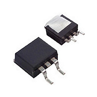
Power MOSFETr
Datasheet
1.MTB33N10E.pdf
(10 pages)
Specifications of MTB33N10E
Number Of Elements
1
Polarity
N
Channel Mode
Enhancement
Drain-source On-res
0.06Ohm
Drain-source On-volt
100V
Gate-source Voltage (max)
±20V
Continuous Drain Current
33A
Power Dissipation
2.5W
Operating Temp Range
-55C to 150C
Operating Temperature Classification
Military
Mounting
Surface Mount
Pin Count
2 +Tab
Package Type
D2PAK
Dc
0106
Lead Free Status / Rohs Status
Not Compliant
Available stocks
Company
Part Number
Manufacturer
Quantity
Price
Company:

Part Number:
MTB33N10E
Manufacturer:
ON
Quantity:
1 537


or an aluminum core board such as Thermal Cladt. Using
a board material such as Thermal Clad, an aluminum core
circuit board, solder paste must be applied to the pads.
Solder stencils are used to screen the optimum amount.
These stencils are typically 0.008 inches thick and may be
made of brass or stainless steel. For packages such as the
SC−59, SC−70/SOT−323, SOD−123, SOT−23, SOT−143,
SOT−223, SO−8, SO−14, SO−16, and SMB/SMC diode
packages, the stencil opening should be the same as the pad
size or a 1:1 registration. This is not the case with the DPAK
and D
solder onto the drain pad, misalignment and/or
“tombstoning” may occur due to an excess of solder. For
these two packages, the opening in the stencil for the paste
should be approximately 50% of the tab area. The opening
for the leads is still a 1:1 registration. Figure 17 shows a
typical stencil for the DPAK and D
temperature of the device. When the entire device is heated
to a high temperature, failure to complete soldering within
a short time could result in device failure. Therefore, the
following items should always be observed in order to
minimize the thermal stress to which the devices are
subjected.
• Always preheat the device.
• The delta temperature between the preheat and
• When preheating and soldering, the temperature of the
• The soldering temperature and time shall not exceed
Another alternative would be to use a ceramic substrate
Prior to placing surface mount components onto a printed
The melting temperature of solder is higher than the rated
soldering should be 100°C or less.*
leads and the case must not exceed the maximum
temperature ratings as shown on the data sheet. When
using infrared heating with the reflow soldering
method, the difference shall be a maximum of 10°C.
260°C for more than 10 seconds.
2
PAK packages. If one uses a 1:1 opening to screen
2
PAK packages. The
SOLDER STENCIL GUIDELINES
SOLDERING PRECAUTIONS
http://onsemi.com
8
board, the power dissipation can be doubled using the same
footprint.
pattern of the opening in the stencil for the drain pad is not
critical as long as it allows approximately 50% of the pad to
be covered with paste.
• When shifting from preheating to soldering, the
• After soldering has been completed, the device should
• Mechanical stress or shock should not be applied
* * Soldering a device without preheating can cause
excessive thermal shock and stress which can result in
damage to the device.
* * Due to shadowing and the inability to set the wave
height to incorporate other surface mount components, the
D
Ç Ç
Ç Ç
Ç Ç Ç Ç
Ç Ç
2
PAK is not recommended for wave soldering.
maximum temperature gradient shall be 5°C or less.
be allowed to cool naturally for at least three minutes.
Gradual cooling should be used as the use of forced
cooling will increase the temperature gradient and
result in latent failure due to mechanical stress.
during cooling.
Figure 17. Typical Stencil for DPAK and
Ç Ç Ç
Ç Ç Ç
Ç Ç Ç
Ç Ç Ç
Ç Ç Ç Ç Ç Ç
D
Ç Ç Ç
Ç Ç Ç
2
PAK Packages
Ç Ç
Ç Ç Ç Ç
SOLDER PASTE
OPENINGS
STENCIL
Related parts for MTB33N10E
Image
Part Number
Description
Manufacturer
Datasheet
Request
R

Part Number:
Description:
ON Semiconductor [VOLTAGE REGULATOR]
Manufacturer:
ON Semiconductor
Datasheet:
Part Number:
Description:
357-036-542-201 CARDEDGE 36POS DL .156 BLK LOPRO
Manufacturer:
ON Semiconductor
Datasheet:
Part Number:
Description:
357-036-542-201 CARDEDGE 36POS DL .156 BLK LOPRO
Manufacturer:
ON Semiconductor
Datasheet:
Part Number:
Description:
357-036-542-201 CARDEDGE 36POS DL .156 BLK LOPRO
Manufacturer:
ON Semiconductor
Datasheet:
Part Number:
Description:
357-036-542-201 CARDEDGE 36POS DL .156 BLK LOPRO
Manufacturer:
ON Semiconductor
Datasheet:
Part Number:
Description:
357-036-542-201 CARDEDGE 36POS DL .156 BLK LOPRO
Manufacturer:
ON Semiconductor
Datasheet:
Part Number:
Description:
357-036-542-201 CARDEDGE 36POS DL .156 BLK LOPRO
Manufacturer:
ON Semiconductor
Datasheet:
Part Number:
Description:
357-036-542-201 CARDEDGE 36POS DL .156 BLK LOPRO
Manufacturer:
ON Semiconductor
Datasheet:
Part Number:
Description:
357-036-542-201 CARDEDGE 36POS DL .156 BLK LOPRO
Manufacturer:
ON Semiconductor
Datasheet:
Part Number:
Description:
357-036-542-201 CARDEDGE 36POS DL .156 BLK LOPRO
Manufacturer:
ON Semiconductor
Datasheet:
Part Number:
Description:
357-036-542-201 CARDEDGE 36POS DL .156 BLK LOPRO
Manufacturer:
ON Semiconductor
Datasheet:
Part Number:
Description:
Manufacturer:
ON Semiconductor
Datasheet:
Part Number:
Description:
Manufacturer:
ON Semiconductor
Datasheet:
Part Number:
Description:
Manufacturer:
ON Semiconductor
Datasheet: