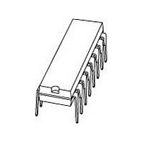
PCF8574P NXP Semiconductors, PCF8574P Datasheet - Page 7

PCF8574P
Manufacturer Part Number
PCF8574P
Description
Manufacturer
NXP Semiconductors
Datasheet
1.PCF8574P.pdf
(24 pages)
Specifications of PCF8574P
Operating Temperature (min)
-40C
Operating Temperature Classification
Industrial
Operating Temperature (max)
85C
Package Type
PDIP
Rad Hardened
No
Lead Free Status / Rohs Status
Compliant
Available stocks
Company
Part Number
Manufacturer
Quantity
Price
Company:
Part Number:
PCF8574P
Manufacturer:
TI
Quantity:
1 870
Part Number:
PCF8574P
Manufacturer:
NXP/恩智浦
Quantity:
20 000
Part Number:
PCF8574P,112
Manufacturer:
NXP/恩智浦
Quantity:
20 000
Company:
Part Number:
PCF8574P-3
Manufacturer:
AFATECH
Quantity:
16 725
Part Number:
PCF8574PW
Manufacturer:
TI/德州仪器
Quantity:
20 000
Company:
Part Number:
PCF8574PWR
Manufacturer:
LT
Quantity:
7 600
Part Number:
PCF8574PWR
Manufacturer:
TI/德州仪器
Quantity:
20 000
Philips Semiconductors
6
The I
different ICs or modules. The two lines are a serial data
line (SDA) and a serial clock line (SCL). Both lines must be
connected to a positive supply via a pull-up resistor when
connected to the output stages of a device. Data transfer
may be initiated only when the bus is not busy.
6.1
One data bit is transferred during each clock pulse. The
data on the SDA line must remain stable during the HIGH
period of the clock pulse as changes in the data line at this
time will be interpreted as control signals (see Fig.5).
2002 Nov 22
handbook, full pagewidth
handbook, full pagewidth
Remote 8-bit I/O expander for I
CHARACTERISTICS OF THE I
2
C-bus is for 2-way, 2-line communication between
Bit transfer
SDA
SCL
TRANSMITTER /
SDA
SCL
RECEIVER
MASTER
START condition
SDA
SCL
S
2
C-BUS
Fig.6 Definition of start and stop conditions.
RECEIVER
SLAVE
Fig.7 System configuration.
data valid
data line
stable;
2
C-bus
Fig.5 Bit transfer.
TRANSMITTER /
RECEIVER
SLAVE
7
allowed
change
of data
6.2
Both data and clock lines remain HIGH when the bus is not
busy. A HIGH-to-LOW transition of the data line, while the
clock is HIGH is defined as the start condition (S).
A LOW-to-HIGH transition of the data line while the clock
is HIGH is defined as the stop condition (P) (see Fig.6).
6.3
A device generating a message is a ‘transmitter’, a device
receiving is the ‘receiver’. The device that controls the
message is the ‘master’ and the devices which are
controlled by the master are the ‘slaves’ (see Fig.7).
Start and stop conditions
System configuration
TRANSMITTER
MASTER
STOP condition
MBC621
P
MBC622
TRANSMITTER /
RECEIVER
SDA
MASTER
SCL
Product specification
PCF8574
MBA605


