NLAS1053US ON Semiconductor, NLAS1053US Datasheet
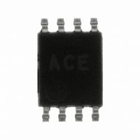
IC SWITCH SPDT US8

NLAS1053US

Manufacturer Part Number
NLAS1053US
Description
IC SWITCH SPDT US8
Manufacturer
ON Semiconductor
Datasheet

Specifications of NLAS1053US

Function
Switch
Circuit
1 x SPDT
On-state Resistance
22 Ohm
Voltage Supply Source
Single Supply
Voltage - Supply, Single/dual (±)
2 V ~ 5.5 V
Current - Supply
1µA
Operating Temperature
-55°C ~ 125°C
Mounting Type
Surface Mount
Package / Case
US8, 8-VSSOP
Lead Free Status / RoHS Status
Contains lead / RoHS non-compliant
Other names
NLAS1053USOSTR

Available stocks

Company
Part Number
Manufacturer
Quantity
Price
Part Number:
NLAS1053US
Quantity:
2 416
Part Number:
NLAS1053USG
Manufacturer:
ON Semiconductor
Quantity:
500
Part Number:
NLAS1053USG
Manufacturer:
ON/安森美
Quantity:
20 000
Company:
Part Number:
NLAS1053USG
Quantity:
3 000
NLAS1053
2:1 Mux/Demux Analog
Switches
with silicon gate CMOS technology. It achieves very high speed
propagation delays and low ON resistances while maintaining CMOS
low power dissipation. The device consists of a single 2:1
Mux/Demux (SPDT), similar to ON Semiconductor’s NLAS4053
analog and digital voltages that may vary across the full power supply
range (from V
allows voltages above V
or disruption of operation of the part, regardless of the operating
voltage.
Features
© Semiconductor Components Industries, LLC, 2006
May, 2006 − Rev. 2
The NLAS1053 is an advanced CMOS analog switch fabricated
The inhibit and select input pins have over voltage protection that
High Speed: t
Low Power Dissipation: I
High Bandwidth, Improved Linearity, and Low RDS
INH Pin Allows a Both Channels ‘OFF’ Condition (With a High)
RDS
Break Before Make Circuitry, Prevents Inadvertent Shorts
Useful For Switching Video Frequencies Beyond 50 MHz
Latchup Performance Exceeds 300 mA
ESD Performance: HBM > 2000 V; MM > 200 V, CDM > 1500 V
Tiny US8 Package, Only 2.1 X 3.0 mm
Pb−Free Package is Available
ON
≅ 25 W, Performance Very Similar to the NLAS4053
CC
COM
GND
INH
N/C
PD
Figure 1. Pin Assignment
to GND).
= 1 ns (Typ) at V
1
2
3
4
CC
up to 7.0 V to be present without damage
CC
= 2 mA (Max) at T
CC
8
7
6 CH1
5
= 5.0 V
V
CH0
Select
CC
A
= 25°C
ON
1
†For information on tape and reel specifications,
NLAS1053US
NLAS1053USG
including part orientation and tape sizes, please
refer to our Tape and Reel Packaging Specifications
Brochure, BRD8011/D.
*Date Code orientation may vary depending
Device
INH
upon manufacturing location.
(Note: Microdot may be in either location)
H
L
L
ORDERING INFORMATION
AC = Specific Device Code
M
G
1
MARKING DIAGRAMS
FUNCTION TABLE
http://onsemi.com
Select
= Date Code*
= Pb−Free Package
H
X
L
(Pb−Free)
8
1
Package
US8
US8
AC M G
Publication Order Number:
G
CASE 493−01
US SUFFIX
Ch 0
OFF
OFF
ON
3000 / Tape & Reel
3000 / Tape & Reel
US8
Shipping
NLAS1053/D
Ch 1
OFF
OFF
ON

Related parts for NLAS1053US

NLAS1053US Summary of contents

Page 1

... ORDERING INFORMATION Device Package Shipping NLAS1053US US8 3000 / Tape & Reel NLAS1053USG US8 3000 / Tape & Reel (Pb−Free) †For information on tape and reel specifications, including part orientation and tape sizes, please refer to our Tape and Reel Packaging Specifications Brochure, BRD8011/D. ...

Page 2

MAXIMUM RATINGS Parameter Positive DC Supply Voltage Digital Input Voltage (Select and Inhibit) Analog Output Voltage ( COM DC Current, Into or Out of Any Pin Storage Temperature Range Lead Temperature from Case for ...

Page 3

DC CHARACTERISTICS − Digital Section (Voltages Referenced to GND) Parameter Condition Minimum High−Level Input Voltage, Select and Inhibit Inputs Maximum Low−Level Input Voltage, Select and Inhibit Inputs Maximum Input Leakage GND IN Current, Select and ...

Page 4

AC ELECTRICAL CHARACTERISTICS Parameter Test Conditions = 300 W, C Turn−On Time R L (Figures 12 and 13) (Figures 4 and 5) INH to Output = 300 W, C Turn−Off Time R L (Figures 12 and 13) (Figures 4 and ...

Page 5

DUT V Output CC 0.1 mF 300 W Switch Select Pin DUT V Output CC 0.1 mF Open 300 W INH Input V DUT Output Open INH Input NLAS1053 V CC Input GND V OUT 35 pF Output GND Figure ...

Page 6

V Output CC 0.1 mF GND 300 W Select Pin 50 W Generator Channel switch control/s test socket is normalized. Off isolation is measured across an off channel. On loss is the bandwidth switch ...

Page 7

I COM(ON) 0.1 I COM(OFF) 0.01 I CH(OFF) 0.001 −55 − TEMPERATURE (°C) Figure 9. Switch Leakage versus Temperature 5 25_C A 0.01 0.1 1 ...

Page 8

1.5 1.0 0 −0 (V) COM Figure 15. Charge Injection versus COM Voltage 100 ...

Page 9

V (VOLTS) COM Figure 21. R versus V and Temperature, ON COM ...

Page 10

... Pb−Free strategy and soldering details, please download the ON Semiconductor Soldering and Mounting Techniques Reference Manual, SOLDERRM/D. ON Semiconductor and are registered trademarks of Semiconductor Components Industries, LLC (SCILLC). SCILLC reserves the right to make changes without further notice to any products herein ...

Related keywords