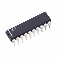
LTC1061ACN Linear Technology, LTC1061ACN Datasheet - Page 14

LTC1061ACN
Manufacturer Part Number
LTC1061ACN
Description
IC FILTER BUILDNG BLK TRPL 20DIP
Manufacturer
Linear Technology
Datasheet
1.LTC1061CNPBF.pdf
(16 pages)
Specifications of LTC1061ACN
Filter Type
Universal Switched Capacitor
Frequency - Cutoff Or Center
35kHz
Number Of Filters
3
Max-order
6th
Voltage - Supply
4.74 V ~ 16 V, ±2.37 V ~ 8 V
Mounting Type
Through Hole
Package / Case
20-DIP (0.300", 7.62mm)
Lead Free Status / RoHS Status
Contains lead / RoHS non-compliant
Available stocks
Company
Part Number
Manufacturer
Quantity
Price
Company:
Part Number:
LTC1061ACN#PBF
Manufacturer:
LT
Quantity:
1 001
W
LTC1061
14
ODES OF OPERATIO
MODE
1b
V
1
2
3
S
(±V)
5.0
5.0
2.5
2.5
5.0
5.0
2.5
2.5
5.0
5.0
2.5
2.5
5.0
5.0
2.5
2.5
V
V
[V
× [R4/(R2 + R4)] + V
V
OS1
OS1
OS2
OS1
(11,17)
[(1/Q) + 1 + || H
[(1/Q) + 1 + R2/R1] – V
(1 + R2/R1 + R2/R3 + R2/R4) – V
4
f
CLK/
100:1
100:1
100:1
100:1
100:1
100:1
100:1
100:1
PIN 3 (18)
50:1
50:1
50:1
50:1
50:1
50:1
50:1
50:1
+
f
V
O
V
OSN
OS1
6
OS2
OLP
Figure 23. Equivalent Input Offsets of 1/3 LTC1061 Filter Building Block
–
[R2/(R2 + R4)]
||] – V
+
–
OS3
NOTCH/HP
OS3
/Q
U
(µV
135
170
100
125
/Q
45
65
30
40
18
20
15
17
57
72
40
50
RMS
OS3
)
3
Table 3. Wideband RMS Noise
(R2/R3)] ×
(12,18)
+
Σ
5
–
(µV
+
Table 4
150
200
100
140
120
160
115
V
BP
RMS
55
65
30
40
57
72
40
50
88
OS2
)
–
PIN 2 (19)
V
+
–
V
V
V
V
OSBP
OS3
OS3
OS3
OS3
(µV
150
200
140
185
100
100
140
130
LP
V
~(V
V
V
– V
85
60
62
80
53
RMS
70
45
42
2
OSN
OSN
OS1
(13,19)
OS3
OSN
+
)
(1 + R4/R1 + R4/R2 + R4/R3) – V
– V
– V
V
(R4/R3)
OS3
– V
OS2
OS2
PIN 1 (20)
OS2
–
V
)(1 + R5/R6)
OSLP
+
–
R1 = R3 for BP Out
Mode 3, R2 = R4, Q = 10
CONDITIONS
Mode 1, R1 = R2 = R3
Q = 1
Mode 1, Q = 10
R1 = R2 for LP Out
Mode 3, R1 = R2 = R3 = R4
Q = 1
R3 = R1 for BP Out
R4 = R1 for LP and HP Out
1
1061 F23
(14,20)
OS2
(R4/R2)
1061fe


