CDB1601-120W-Z Cirrus Logic Inc, CDB1601-120W-Z Datasheet - Page 10
CDB1601-120W-Z
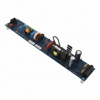
Manufacturer Part Number
CDB1601-120W-Z
Description
High-efficiency PFC Demo. Board
Manufacturer
Cirrus Logic Inc
Series
-r
Datasheets
1.CDB150X-01-Z.pdf
(2 pages)
2.CDB1601-120W-Z.pdf
(24 pages)
3.CDB1601-120W-Z.pdf
(16 pages)
Specifications of CDB1601-120W-Z
Silicon Manufacturer
Cirrus Logic
Kit Application Type
Power Management
Application Sub Type
Power Factor Correction (PFC)
Kit Contents
Board, Datasheet
Design Resources
CS150x/160x PCB Layout Guidelines
Featured Product
CS1501/CS1601 Power Factor Correction IC Controllers
Main Purpose
Power Management, Power Factor Correction
Embedded
No
Utilized Ic / Part
CS1601
Primary Attributes
108 ~ 305 VAC Input, 460V 120W Output
Secondary Attributes
Ballast Control, Up to 2 T5 Lamps
Lead Free Status / Rohs Status
Lead free / RoHS Compliant


5.2 Startup vs. Normal Operation Mode
The CS1601 has two discrete operation modes: startup and
normal. Startup mode will be activated when V
90% of nominal value, V
reaches 100% of nominal value, as shown in Figure 15.
Startup mode is activated during initial system power-up. Any
V
cause the system to enter startup mode until V
back into regulation.
Startup mode is defined as a surge of current delivering
maximum power to the output regardless of the load. During
every active switch cycle, the 'ON' time is calculated to drive a
constant peak current over the entire line cycle. However, the
'OFF' time is calculated based on the DCM/CCM boundary
equation.
5.3 Burst Mode
Burst mode is utilized to improve system efficiency when the
system output power (P
implemented by intermittently disabling the PFC over a full
half-line period under light-load conditions, as shown in
Figure 16.
10
100%
90%
link
V
[V]
link
drop to less than V
V
[V]
[W]
P
in
o
Figure 15. Startup and Normal Modes
Figure 16. Burst Modes
V
Normal
Mode
in
O(startup)
O(startup)
Burst Threshold
o
) is <5% of nominal. Burst mode is
Burst Mode
Disable
, such as a load change, can
PFC
Active
and remains active until V
Normal
Mode
link
link
t [ms]
t [ms]
t [ms]
is less than
FET
V
is brought
gs
link
5.4 Output Power and PFC Boost Inductor
In normal operating mode, the nominal output power is
estimated by the following equation.
where:
P
V
V
f
L
Equation 1 is provided for explanation purposes only. Using
substituted required design values for V
following equation:
Changing the value for the V
Solving Equation 2 for the PFC boost inductor L
following equation:
If a value of the boost inductor other than that obtained from
Equation 3 above is used, the total output power capability as
well as the minimum input voltage threshold will differ
according to Equation 2. Note that if the input voltage drops
below 108 Vrms and the inductance value is < L
voltage V
Figure 17. Relative Effects of Varying Boost Inductance
max
B
in(min)
o
link
P
P
L
o
o
B
=
=
=
by the PFC algorithm)
against boost inductor tolerances.
rated output power of the system
efficiency of the boost converter (estimated as 100%
minimum RMS line voltage measured after the
rectifier and EMI filter. V
108 Vrms depending on the AC Line Voltage
operating range.
nominal PFC output voltage; V
V
V
maximum switching frequency; for the CS1601
f
boost inductor specified by rated power requirement
margin factor to guarantee rated output power (P
link
max
in(min)
i n ( m i n )
will drop below 460V and fall out of regulation.
= 70kHz and the CS1601H f
= 108Vrms
V
108V
108V
in min
= 9 0 Vr m s
108
2
2
2
------------------------------------------------------------ -
2 70kHz P
------------------------------------------------------------ -
2 70kHz
V
460V
link
460V
AC(rms)
V
-------------------------------------------------------- -
2 f
link
voltage is not recommended.
o r
in(min)
L < L
L > L
–
L = L
–
max
–
108V
V
108V
V
B
B
in min
B
is equal to 90Vrms or
l i n k
link
L
o
L
B
max
B
and f
link
= 4 6 0 V
460V
460V
V
305
= 100kHz
2
= 400V when
2
link
max
2
DS931PP6
B
B
gives the
, the link
gives the
w h e n
[Eq.1]
[Eq.2]
[Eq.3]
o
)
Related parts for CDB1601-120W-Z
Image
Part Number
Description
Manufacturer
Datasheet
Request
R

Part Number:
Description:
Development Kit
Manufacturer:
Cirrus Logic Inc
Datasheet:
Part Number:
Description:
Development Kit
Manufacturer:
Cirrus Logic Inc
Datasheet:


Part Number:
Description:
High-efficiency PFC + Fluorescent Lamp Driver Reference Design
Manufacturer:
Cirrus Logic Inc
Datasheet:
Part Number:
Description:
Development Kit
Manufacturer:
Cirrus Logic Inc
Datasheet:
Part Number:
Description:
Development Kit
Manufacturer:
Cirrus Logic Inc
Datasheet:

Part Number:
Description:
Development Kit
Manufacturer:
Cirrus Logic Inc
Datasheet:
Part Number:
Description:
Development Kit
Manufacturer:
Cirrus Logic Inc
Datasheet:
Part Number:
Description:
Development Kit
Manufacturer:
Cirrus Logic Inc
Datasheet:
Part Number:
Description:
Development Kit
Manufacturer:
Cirrus Logic Inc
Datasheet:

Part Number:
Description:
EVALUATION BOARD FOR CS8427
Manufacturer:
Cirrus Logic Inc
Datasheet:

Part Number:
Description:
BOARD EVAL FOR CS8416 RCVR
Manufacturer:
Cirrus Logic Inc
Datasheet:

Part Number:
Description:
EVALUATION BOARD FOR CS8420
Manufacturer:
Cirrus Logic Inc
Datasheet:

Part Number:
Description:
KIT DEVELOPMENT EP9315 ARM9
Manufacturer:
Cirrus Logic Inc
Datasheet:

Part Number:
Description:
KIT DEVELOPMENT EP9302 ARM9
Manufacturer:
Cirrus Logic Inc
Datasheet: