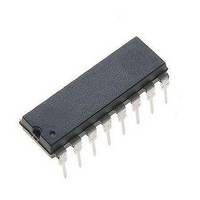
MC44603P ON Semiconductor, MC44603P Datasheet - Page 17

MC44603P
Manufacturer Part Number
MC44603P
Description
Other Power Management Voltage/Current PWM
Manufacturer
ON Semiconductor
Type
PWM Mode Controllerr
Datasheet
1.MC44603DWR2.pdf
(24 pages)
Specifications of MC44603P
Input Voltage Range
18 V
Mounting Style
Through Hole
Package / Case
PDIP-16
Lead Free Status / Rohs Status
Lead free / RoHS Compliant
Available stocks
Company
Part Number
Manufacturer
Quantity
Price
Part Number:
MC44603P
Manufacturer:
MOTOROLA/摩托罗拉
Quantity:
20 000
Company:
Part Number:
MC44603P2
Manufacturer:
ON
Quantity:
9 800
Consequently:
where:
and
arrangement is not activated, the operating frequency can be
obtained from the graph in Figure 2.
NOTE: The output is disabled by the signal V
V
Synchronization and Demagnetization Blocks
output must be low. Reset is activated by the L
during the discharge phase. To restart, the L
(refer to Figure 35). To perform this, the demagnetization
signal and the synchronization must be low.
•
that compare the synchronization signal (external) to 0.7 and
3.7 V (typical values). The comparators’ outputs are
connected to the input of an AND gate so that the final output
of the block should be:
synchronized low level pulses have to be generated on the
output of the synchronization block. If synchronization is
not required, the Pin 9 must be connected to the ground.
•
saturation of the transformer core, or demagnetization,
consists in using the auxiliary winding voltage. This voltage
is:
CT
T
T
T
DV is the oscillator peak−to−peak value
I
T
I
So, as f
To enable the output, the L
The synchronization block consists of two comparators
− high when 0.7 < SYNC < 3.7 V
− low in the other cases.
As a low level is necessary to enable the output,
In flyback applications, a good means to detect magnetic
− negative during the on−time,
− positive during the off−time,
− equal to zero for the dead−time with generally some
−
Synchronization:
Demagnetization:
charge
discharge
charge
charge
discharge
discharge
ringing (refer to Figure 38).
is lower than 1.0 V (refer to Figure 31).
Oscillator
Output Buffer
is the oscillator charge current
= C
is the oscillator charge time
S
is the oscillator discharge current
= C
is the oscillator discharge time
T
= 1 /(T
Figure 37. Synchronization
x DV/I
T
x DV/I
charge
charge
discharge
+ T
discharge
OSC
latch complementary
3.7 V
0.7 V
) when the Regul
OSC
OSC prot
has to be set
disch
Sync
9
http://onsemi.com
output
when
17
consists of a comparator that can compare the auxiliary
winding voltage to a reference that is typically equal to
65 mV.
applied voltages while an active clamping system limits the
negative voltages to typically −0.33 V. This negative clamp
level is sufficient to avoid the substrate diode switching on.
incorporated in order to keep the demagnetization block
output level low as soon as a voltage lower than 65 mV is
detected and as long as a new restart is produced (high level
on the output) (refer to Figure 39). This process prevents
ringing on the signal at Pin 8 from disrupting the
demagnetization detection. This results in a very accurate
demagnetization detection.
connected to the output, disabling it during the
demagnetization phase (refer to Figure 34).
NOTE: The demagnetization detection can be inhibited by
connecting Pin 8 to the ground.
Standby
•
That is why, the MC44603A demagnetization detection
A diode D has been incorporated to clamp the positive
In addition to the comparator, a latch system has been
The demagnetization block output is also directly
V
Power Losses in a Classical Flyback Structure
Pin 8
Oscillator
V
Demag Out
Figure 38. Demagnetization Detection
Figure 39. Demagnetization Block
Buffer
On-Time
Output
Off-Time
R
Demag
S
C Dem
Q
Zero Current
Detection
Dead-Time
65 mV
Clamping System
Negative Active
V
CC
D
0.75 V
65 mV
-0.33 V
8


