KSZ8893MBL Micrel Inc, KSZ8893MBL Datasheet
KSZ8893MBL
Specifications of KSZ8893MBL
Available stocks


Related parts for KSZ8893MBL

KSZ8893MBL Summary of contents
Page 1
General Description The KSZ8893MQL/MBL, a highly integrated layer 2 managed switch, is designed for low port count, cost-sensitive 10/100 Mbps switch systems. It offers an extensive feature set that includes rate limiting, tag/port-based VLAN, QoS priority, management, management information base ...
Page 2
Features • Proven Integrated 3-Port 10/100 Ethernet Switch – 3rd generation switch with three MACs and two PHYs fully compliant with IEEE 802.3u standard – Non-blocking switch fabric assures fast packet delivery by utilizing an 1K MAC address lookup table ...
Page 3
... Recommend connecting a 100ohm resistor between VDDC and 3.3V power rail. 1.5 11/05/07 Add the KSZ8893MBL BGA device information. 11/26/07 Modify the Hold time, Output valid in table 25, 26 and Figure 25,26 of MII interface timing. 12/10/07 Add the I2C timing diagram and parameters in Figure and Table 28. ...
Page 4
... Contents List of Figures...................................................................................................................................... 8 List of Tables ....................................................................................................................................... 9 Pin Description and I/O Assignment of KSZ8893MQL .................................................................... 10 Ball Description and I/O Assignment of KSZ8893MBL ................................................................... 19 Pin Configuration............................................................................................................................... 26 Functional Overview: Physical Layer Transceiver .......................................................................... 28 100BASE-TX Transmit.........................................................................................................................................................28 100BASE-TX Receive ..........................................................................................................................................................28 PLL Clock Synthesizer........................................................................................................................................................28 Scrambler/De-scrambler (100BASE-TX Only) ...................................................................................................................29 100BASE-FX Operation.......................................................................................................................................................29 100BASE-FX Signal Detection............................................................................................................................................29 100BASE-FX Far-End Fault.................................................................................................................................................29 10BASE-T Transmit ...
Page 5
QoS Priority Support...........................................................................................................................................................48 Port-Based Priority..............................................................................................................................................................48 802.1p-Based Priority..........................................................................................................................................................48 DiffServ-Based Priority .......................................................................................................................................................49 Rate Limiting Support .........................................................................................................................................................49 Unicast MAC Address Filtering..........................................................................................................................................49 Configuration Interface ....................................................................................................................................................... Master Serial Bus Configuration .............................................................................................................................. Slave Serial Bus Configuration ................................................................................................................................51 SPI Slave Serial ...
Page 6
Register 18 (0x12): Port 1 Control 2 ..............................................................................................................................71 Register 34 (0x22): Port 2 Control 2 ..............................................................................................................................71 Register 50 (0x32): Port 3 Control 2 ..............................................................................................................................71 Register 19 (0x13): Port 1 Control 3 ..............................................................................................................................72 Register 35 (0x23): Port 2 Control 3 ..............................................................................................................................72 ...
Page 7
Register 114 (0x72): MAC Address Register 2 ..............................................................................................................89 Register 115 (0x73): MAC Address Register 3 ..............................................................................................................89 Register 116 (0x74): MAC Address Register 4 ..............................................................................................................89 Register 117 (0x75): MAC Address Register 5 ..............................................................................................................89 Register 118 (0x76): User Defined Register 1 ...............................................................................................................90 ...
Page 8
List of Figures Figure 1. Typical Straight Cable Connection........................................................................................................................................ 31 Figure 2. Typical Crossover Cable Connection.................................................................................................................................... 32 Figure 3. Auto-Negotiation and Parallel Operation .............................................................................................................................. 33 Figure 4. Destination Address Lookup Flow Chart, Stage 1 ................................................................................................................ 36 Figure 5. Destination Address ...
Page 9
List of Tables Table 1. FX and TX Mode Selection .................................................................................................................................................... 29 Table 2. MDI/MDI-X Pin Definitions ..................................................................................................................................................... 30 Table 3. MII Signals............................................................................................................................................................................. 39 Table 4: RMII Signal Description ......................................................................................................................................................... 40 Table 5: RMII Signal Connections ....................................................................................................................................................... 41 Table 6. ...
Page 10
Pin Description and I/O Assignment of KSZ8893MQL Pin Number Pin Name 1 P1LED2 2 P1LED1 3 P1LED0 Note: 1. Ipu/O = Input with internal pull-up during reset, output pin otherwise. December 2007 (1) Type Description Ipu/O Port 1 LED Indicators ...
Page 11
Pin Number Pin Name 4 P2LED2 5 P2LED1 6 P2LED0 7 DGND 8 VDDIO Note Power supply. Gnd = Ground. Ipu/O = Input with internal pull-up during reset, output pin otherwise. December 2007 (1) Type Description Ipu/O ...
Page 12
... Note: Internal pull-down is weak; it will not turn ON the LED. See description in pin 4. Gnd Digital ground P 1.2V digital VDD Provides V to KSZ8893MBL’s input power pins: V OUT_1V2 (pin 63), V (pins 91 and 123), and V DDC 57 recommended the pin should be connected to 3.3V power rail by a 100ohm resistor for the internal LDO application ...
Page 13
Pin Number Pin Name 26 RMII_EN 27 HWPOVR 28 P2MDIXDIS 29 P2MDIX 30 P1ANEN 31 P1SPD 32 P1DPX 33 P1FFC PWRDN 37 AGND 38 VDDA 39 AGND 40 MUX1 41 MUX2 Note ...
Page 14
Pin Number Pin Name 42 AGND 43 VDDA 44 FXSD1 45 RXP1 46 RXM1 47 AGND 48 TXP1 49 TXM1 50 VDDATX 51 VDDARX 52 RXM2 53 RXP2 54 AGND 55 TXM2 56 TXP2 57 VDDA 58 AGND 59 TEST1 ...
Page 15
Pin Number Pin Name 70 LEDSEL0 71 SMTXEN 72 SMTXD3 73 SMTXD2 74 SMTXD1 75 SMTXD0 76 SMTXER 77 SMTXC / REFCLK 78 DGND 79 VDDIO 80 SMRXC 81 SMRXDV 82 SMRXD3 83 SMRXD2 84 SMRXD1 85 SMRXD0 86 SCOL ...
Page 16
... Note: an external pull-up is needed on this pin when use. I SPI slave mode: chip select (active low) When SPIS_N is high, the KSZ8893MBL is deselected and SPIQ is held in high impedance state. A high-to-low transition is used to initiate SPI data transfer. See description in pins 100 and 101. Note: an external pull-up is needed on this pin when use ...
Page 17
... SCL SDA SPIS_N [PS1, PS0] = [1, 1] – SMI-mode In this mode, the KSZ8893MBL provides access to all its internal 8-bit registers through its MDC and MDIO pins. Note: When (PS1, PS0) ≠ (1,1), the KSZ8893MBL provides access to its 16-bit MIIM registers through its MDC and MDIO pins. ...
Page 18
Pin Number Pin Name 104 UNUSED 105 UNUSED 106 DGND 107 VDDIO 108 UNUSED 109 UNUSED 110 UNUSED 111 UNUSED 112 UNUSED 113 UNUSED 114 UNUSED 115 UNUSED 116 UNUSED 117 UNUSED 118 UNUSED 119 UNUSED 120 UNUSED 121 UNUSED ...
Page 19
... Ball Description and I/O Assignment of KSZ8893MBL Ball Number Ball Name C10 P1LED2 B10 P1LED1 A10 P1LED0 Note: 1. Ipu/O = Input with internal pull-up during reset, output pin otherwise. December 2007 (1) Type Ball Function Description Ipu/O Port 1 LED Indicators (apply to all modes of operation, except Repeater Mode) ...
Page 20
Ball Number Ball Name C9 P2LED2 B9 P2LED1 A9 P2LED0 C8 ADVFC B8 P2ANEN December 2007 (1) Type Ball Function Description Ipu/O Port 2 LED Indicators (apply to all modes of operation, except Repeater Mode) Ipu/O Ipu/O P2LED3 P2LED2 P2LED1 ...
Page 21
Ball Number Ball Name A8 P2SPD B7 P2DPX A7 P2FFC B6 P2LED3 A6 LEDSEL1 B5 P1LED3 A5 RMII_EN B4 HWPOVR A4 P2MDIXDIS B3 P2MDIX A3 P1ANEN B2 P1SPD A2 P1DPX December 2007 (1) Type Ball Function Description Ipd 1 = ...
Page 22
Ball Number Ball Name A1 P1FFC B1 PWRDN C3 FXSD1 C1 RXP1 C2 RXM1 D1 TXP1 D2 TXM1 F2 RXM2 F1 RXP2 G2 TXM2 G1 TXP2 H2 ISET RST_N J2 LEDSEL0 K2 SMTXEN J3 SMTXD3 ...
Page 23
... Note: an external pull-up is needed on this pin when use. I SPI slave mode: chip select (active low) When SPIS_N is high, the KSZ8893MBL is deselected and SPIQ is held in high impedance state. A high-to-low transition is used to initiate SPI data transfer. See description in pins 100 and 101. Note: an external pull-up is needed on this pin when use ...
Page 24
... SCL SDA SPIS_N [PS1, PS0] = [1, 1] – SMI-mode In this mode, the KSZ8893MBL provides access to all its internal 8-bit registers through its MDC and MDIO pins. Note: When (PS1, PS0) ≠ (1,1), the KSZ8893MBL provides access to its 16-bit MIIM registers through its MDC and MDIO pins. ...
Page 25
Ball Number Ball Name E3, F3, G3 VDDA C6, C7, F8, G8, VDDIO H4 VDDATX E2 VDDARX D4, D5, D6, D7, GND E4, E5, E6, E7, F4, F5, F6, F7, G4, G5, G6, G7 D3, H3 ...
Page 26
Pin Configuration 103 UNUSED 104 UNUSED 105 UNUSED 106 DGND 107 VDDIO 108 UNUSED 109 UNUSED 110 UNUSED 111 UNUSED 112 UNUSED 113 UNUSED 114 UNUSED 115 UNUSED 116 UNUSED 117 UNUSED 118 UNUSED 119 UNUSED 120 UNUSED 121 UNUSED ...
Page 27
... GND GND VDDA GND GND GND VDDA GND GND GND VDD VDD NC VDDC TXD3 TXD1 TXER RXDV TXD2 TXD0 TXC RXC KSZ8893MBL 100-Ball LFBGA (Top View FFC SPD LED0 LED0 P2 P2AN P2 P1 DPX EN LED1 LED1 VDD ADV LED2 LED2 TEST SCAN ...
Page 28
Functional Description The KSZ8893MQL/MBL contains two 10/100 physical layer transceivers and three MAC units with an integrated Layer 2 managed switch. The KSZ8893MQL/MBL has the flexibility to reside in either a managed or unmanaged design managed design, the ...
Page 29
Scrambler/De-scrambler (100BASE-TX Only) The purpose of the scrambler is to spread the power spectrum of the signal to reduce electromagnetic interference (EMI) and baseline wander. Transmitted data is scrambled through the use of an 11-bit wide linear feedback shift register ...
Page 30
Receive On the receive side, input buffers and level detecting squelch circuits are employed. A differential input receiver circuit and a phase-locked loop (PLL) perform the decoding function. The Manchester-encoded data stream is separated into clock signal and NRZ ...
Page 31
Straight Cable A straight cable connects an MDI device to an MDI-X device MDI-X device to an MDI device. The following diagram depicts a typical straight cable connection between a NIC card (MDI) and a switch, or hub ...
Page 32
Crossover Cable A crossover cable connects an MDI device to another MDI device MDI-X device to another MDI-X device. The following diagram shows a typical crossover cable connection between two switches or hubs (two MDI-X devices). 10/100 Ethernet ...
Page 33
Start Auto Negotiation Force Link Setting Yes Bypass Auto Negotiation and Set Link Mode Figure 3. Auto-Negotiation and Parallel Operation December 2007 N Parallel Operation o Attempt Auto Listen for 100BASE-TX Negotiation Idles Join Flow Link Mode Set ? Yes ...
Page 34
LinkMD Cable Diagnostics The LinkMD feature utilizes time domain reflectometry (TDR) to analyze the cabling plant for common cabling problems such as open circuits, short circuits and impedance mismatches. LinkMD works by sending a pulse of known amplitude and duration ...
Page 35
Functional Overview: MAC and Switch Address Lookup The internal lookup table stores MAC addresses and their associated information. It contains a 1K unicast address table plus switching information. The KSZ8893MQL/MBL is guaranteed to learn 1K addresses and distinguishes itself from ...
Page 36
PTF1= NULL Search complete. Get PTF1 from Static MAC Table Search complete. Get PTF1 from Dynamic MAC Table Figure 4. Destination Address Lookup Flow Chart, Stage 1 December 2007 Start - Search VLAN table NO VLAN ID - Ingress VLAN ...
Page 37
Spanning Tree Process IGMP Process Port Mirror Process Port VLAN Membership Check Figure 5. Destination Address Resolution Flow Chart, Stage 2 The KSZ8893MQL/MBL will not forward the following packets: 1. Error packets These include framing errors, Frame Check Sequence (FCS) ...
Page 38
Switching Engine The KSZ8893MQL/MBL features a high-performance switching engine to move data to and from the MACs’ packet buffers. It operates in store and forward mode, while the efficient switching mechanism reduces overall latency. The switching engine has a 32kB ...
Page 39
If the port has packets to send during a backpressure situation, the carrier sense type backpressure is interrupted and those packets are transmitted instead. If there are no additional packets to send, carrier sense type backpressure is reactivated ...
Page 40
... MAC device. Since the switch filters error frames, these MII error signals are not used by the KSZ8893MBL. So, for PHY mode operation, if the device interfacing with the KSZ8893MBL has an MRXER input pin, it needs to be tied low. And, for MAC mode operation, if the device interfacing with the KSZ8893MQL/MBL has an MTXER input pin, it also needs to be tied low ...
Page 41
The KSZ8893MQL/MBL filters error frames, and thus does not implement the RX_ER output signal. To detect error frames from RMII PHY devices, the SMTXER input signal of the KSZ8893MQL/MBL is connected to the RXER output signal of the RMII PHY ...
Page 42
The SNI interface is a bit wide data interface and therefore runs at the network bit rate (not encoded). An additional signal on the transmit side indicates when data is valid. Similarly, the receive side has an indicator that conveys ...
Page 43
Serial Management Interface (SMI) The SMI is the KSZ8893MQL/MBL non-standard MIIM interface that provides access to all KSZ8893MQL/MBL configuration registers. This interface allows an external device to completely monitor and control the states of the KSZ8893MQL/MBL. The SMI interface consists ...
Page 44
Advanced Switch Functions Spanning Tree Support To support spanning tree, port 3 is designated as the processor port. The other ports (port 1 and port 2) can be configured in one of the five spanning tree states via “transmit enable”, ...
Page 45
Special Tagging Mode Special Tagging Mode is designed for spanning tree protocol IGMP snooping and is flexible for use in other applications. Special Tagging, similar to 802.1Q Tagging, requires software to change network drivers to insert/modify/strip/interpret the special tag. This ...
Page 46
For packets from regular ports (port 1 & port 2) to port 3, the port mask is used to tell the processor which port the packets were received on, defined as follows: “0001”, packet from port 1 “0010”, packet from ...
Page 47
Port Mirroring Support KSZ8893MQL/MBL supports “Port Mirroring” comprehensively as: “receive only” mirror on a port All the packets received on the port are mirrored on the sniffer port. For example, port 1 is programmed to be “receive sniff” and port ...
Page 48
FID+SA found in Dynamic MAC Table? No Yes Advanced VLAN features, such as “Ingress VLAN filtering” and “Discard Non PVID packets” are also supported by the KSZ8893MQL/MBL. These features can be set on a per port basis, and are defined ...
Page 49
The KSZ8893MQL/MBL provides the option to insert or remove the priority tagged frame's header at each individual egress port. This header, consisting of the 2 bytes VLAN Protocol ID (VPID) and the 2-byte Tag Control Information field (TCI), is also ...
Page 50
This function is useful in preventing the broadcast of unicast packets that could degrade the quality of the port in applications such as voice over Internet Protocol (VoIP). Configuration Interface The KSZ8893MQL/MBL can operate as both a managed switch and ...
Page 51
I C Slave Serial Bus Configuration In managed mode, the KSZ8893MQL/MBL can be configured device (external controller/CPU) has complete programming access to the KSZ8893MQL/MBL’s 142 registers. Programming access includes the Global Registers, Port Registers, Advanced Control ...
Page 52
The following is a sample procedure for programming the KSZ8893MQL/MBL using the SPI bus the board level, connect the KSZ8893MQL/MBL pins as follows: KSZ8893MQL/MBL Pin # Enable SPI slave mode by setting the ...
Page 53
SPIS_N SPIC SPID SPIQ READ COMMAND SPIS_N SPIC SPID SPIQ WRITE COMMAND SPIS_N SPIC SPID SPIQ Byte 2 SPIS_N SPIC SPID SPIQ READ COMMAND SPIS_N ...
Page 54
Loopback Support The KSZ8893MQL/MBL provides loopback support for remote diagnostic of failure. In loopback mode, the speed at both PHY ports needs to be set to 100BASE-TX. Two types of loopback are supported: Far-end Loopback and Near-end (Remote) Loopback. Far-end ...
Page 55
Near-end (Remote) Loopback Near-end (Remote) loopback is conducted at either PHY port 1 or PHY port 2.of the KSZ8893MQL/MBL. The loopback path starts at the PHY port’s receive inputs (RXPx/RXMx), wraps around at the same PHY port’s PMD/PMA, and ends ...
Page 56
MII Management (MIIM) Registers The MIIM interface is used to access the MII PHY registers defined in this section. The SPI, I interfaces can also be used to access some of these registers. The latter three interfaces use a different ...
Page 57
PHY1 Register 0 (PHYAD = 0x1, REGAD = 0x0): MII Basic Control PHY2 Register 0 (PHYAD = 0x2, REGAD = 0x0): MII Basic Control Bit Name R/W 15 Soft reset RO 14 Loopback R/W 13 Force 100 R ...
Page 58
PHY1 Register 1 (PHYAD = 0x1, REGAD = 0x1): MII Basic Status PHY2 Register 1 (PHYAD = 0x2, REGAD = 0x1): MII Basic Status Bit Name R capable RO 14 100 Full RO capable 13 100 Half RO ...
Page 59
PHY1 Register 4 (PHYAD = 0x1, REGAD = 0x4): Auto-Negotiation Advertisement Ability PHY2 Register 4 (PHYAD = 0x2, REGAD = 0x4): Auto-Negotiation Advertisement Ability Bit Name R/W 15 Next page RO 14 Reserved RO 13 Remote fault RO 12-11 Reserved ...
Page 60
PHY1 Register 29 (PHYAD = 0x1, REGAD = 0x1D): LinkMD Control/Status PHY2 Register 29 (PHYAD = 0x2, REGAD = 0x1D): LinkMD Control/Status Bit Name R/W 15 Vct_enable R/W (SC) 14-13 Vct_result RO 12 Vct 10M Short RO 11-9 Reserved RO ...
Page 61
Register Map: Switch & PHY (8-bit registers) Global Registers Register (Decimal) Register (Hex) 0-1 0x00-0x01 2-15 0x02-0x0F Port Registers Register (Decimal) Register (Hex) 16-29 0x10-0x1D 30-31 0x1E-0x1F 32-45 0x20-0x2D 46-47 0x2E-0x2F 48-57 0x30-0x39 58-62 0x3A-0x3E 63 0x3F 64-95 0x40-0x5F Advanced ...
Page 62
Register 1 (0x01): Chip ID1 / Start Switch Bit Name R/W 7-4 Chip ID RO 3-1 Revision Start Switch RW Register 2 (0x02): Global Control 0 Bit Name R/W 7 New Back-off R/W Enable 6-4 Reserved R/W ...
Page 63
Register 3 (0x03): Global Control 1 Bit Name R/W 7 Pass All R/W Frames 6 Reserved R/W 5 IEEE 802.3x R/W Transmit Direction Flow Control Enable 4 IEEE 802.3x R/W Receive Direction Flow Control Enable 3 Frame Length R/W Field ...
Page 64
Register 4 (0x04): Global Control 2 (continued) Bit Name R/W 4 Flow Control R/W and Back Pressure Fair Mode 3 No Excessive R/W Collision Drop 2 Huge Packet R/W Support 1 Legal R/W Maximum Packet Size Check Enable 0 Priority ...
Page 65
Register 5 (0x05): Global Control 3 (continued) Bit Name R/W 3 Weighted R/W Fair Queue Enable 2-1 Reserved R/W 0 Sniff Mode R/W Select Register 6 (0x06): Global Control 4 Bit Name R/W 7 Repeater R/W Mode 6 Switch MII ...
Page 66
Register 6 (0x06): Global Control 4 (continued) Bit Name R/W 4 Switch MII R/W 10BT 3 Null VID R/W Replacement 2-0 Broadcast R/W Storm Protection (1) Rate Bit [10:8] Register 7 (0x07): Global Control 5 Bit Name R/W 7-0 Broadcast ...
Page 67
Register 11 (0x0B): Global Control 9 Bit Name R/W Description 7 LEDSEL1 R/W LED mode select See description in bit 1 of this register. 6-5 Reserved R/W Reserved Do not change the default values. 4 Reserved R/W Testing mode. Set ...
Page 68
Register 13 (0x0D): Global Control 11 Bit Name R/W Description 7-6 Tag_0x7 R/W IEEE 802.1p mapping. The value in this field is used as the frame’s priority when its IEEE 802.1p tag has a value of 0x7. 5-4 Tag_0x6 R/W ...
Page 69
Register 16 (0x10): Port 1 Control 0 Register 32 (0x20): Port 2 Control 0 Register 48 (0x30): Port 3 Control 0 Bit Name ...
Page 70
Register 17 (0x11): Port 1 Control 1 Register 33 (0x21): Port 2 Control 1 Register 49 (0x31): Port 3 Control 1 Bit Name R/W 7 Sniffer Port R/W 6 Receive Sniff R/W 5 Transmit Sniff R/W 4 Double Tag R/W ...
Page 71
Register 18 (0x12): Port 1 Control 2 Register 34 (0x22): Port 2 Control 2 Register 50 (0x32): Port 3 Control 2 Bit Name R/W 7 Reserved R/W 6 Ingress VLAN R/W Filtering 5 Discard non R/W PVID Packets 4 Force ...
Page 72
Register 19 (0x13): Port 1 Control 3 Register 35 (0x23): Port 2 Control 3 Register 51 (0x33): Port 3 Control 3 Bit Name R/W 7-0 Default Tag R/W [15:8] Register 20 (0x14): Port 1 Control 4 Register 36 (0x24): Port ...
Page 73
Register 22 (0x16): Port 1 Control 6 Register 38 (0x26): Port 2 Control 6 Register 54 (0x36): Port 3 Control 6 Bit Name R/W 7-4 Ingress Pri1 R/W Rate 3-0 Ingress Pri0 R/W Rate December 2007 Description Ingress data rate ...
Page 74
Register 23 (0x17): Port 1 Control 7 Register 39 (0x27): Port 2 Control 7 Register 55 (0x37): Port 3 Control 7 Bit Name R/W 7-4 Ingress Pri3 R/W Rate 3-0 Ingress Pri2 R/W Rate December 2007 Description Ingress data rate ...
Page 75
Register 24 (0x18): Port 1 Control 8 Register 40 (0x28): Port 2 Control 8 Register 56 (0x38): Port 3 Control 8 Bit Name R/W 7-4 Egress Pri1 R/W Rate 3-0 Egress Pri0 R/W Rate December 2007 Description Egress data rate ...
Page 76
Register 25 (0x19): Port 1 Control 9 Register 41 (0x29): Port 2 Control 9 Register 57 (0x39): Port 3 Control 9 Bit Name R/W 7-4 Egress Pri3 R/W Rate 3-0 Egress Pri2 R/W Rate December 2007 Description Egress data rate ...
Page 77
Note: Most of the contents in registers 26-31 and registers 42-47 for ports 1 and 2, respectively, can also be accessed with the MIIM PHY registers. Register 26 (0x1A): Port 1 PHY Special Control/Status Register 42 (0x2A): Port 2 PHY ...
Page 78
Register 28 (0x1C): Port 1 Control 12 Register 44 (0x2C): Port 2 Control 12 Register 60 (0x3C): Reserved, not applied to port 3 Bit Name R/W 7 Auto R/W Negotiation Enable 6 Force Speed R/W 5 Force Duplex R/W 4 ...
Page 79
Register 29 (0x1D): Port 1 Control 13 Register 45 (0x2D): Port 2 Control 13 Register 61 (0x3D): Reserved, not applied to port 3 Bit Name R/W 7 LED Off R/W 6 Txdis R/W 5 Restart AN R/W 4 Disable Far- ...
Page 80
Register 30 (0x1E): Port 1 Status 0 Register 46 (0x2E): Port 2 Status 0 Register 62 (0x3E): Reserved, not applied to port 3 Bit Name R/W MDI-X Status Done 6 RO Link Good 5 RO Partner Flow ...
Page 81
Register 31 (0x1F): Port 1 Status 1 (continued) Register 47 (0x2F): Port 2 Status 1 (continued) Register 63 (0x3F): Port 3 Status 1 (continued) Bit Name R/W 2 Operation RO Speed 1 Operation RO Duplex 0 Far-end Fault RO Advanced ...
Page 82
Register 97 (0x61): TOS Priority Control Register 1 Bit Name R/W 7-6 DSCP[15:14] R/W 5-4 DSCP[13:12] R/W 3-2 DSCP[11:10] R/W 1-0 DSCP[9:8] R/W Register 98 (0x62): TOS Priority Control Register 2 Bit Name R/W 7-6 DSCP[23:22] R/W 5-4 DSCP[21:20] R/W ...
Page 83
Register 99 (0x63): TOS Priority Control Register 3 Bit Name R/W 7-6 DSCP[31:30] R/W 5-4 DSCP[29:28] R/W 3-2 DSCP[27:26] R/W 1-0 DSCP[25:24] R/W Register 100 (0x64): TOS Priority Control Register 4 Bit Name R/W 7-6 DSCP[39:38] R/W 5-4 DSCP[37:36] R/W ...
Page 84
Register 101 (0x65): TOS Priority Control Register 5 Bit Name R/W 7-6 DSCP[47:46] R/W 5-4 DSCP[45:44] R/W 3-2 DSCP[43:42] R/W 1-0 DSCP[41:40] R/W Register 102 (0x66): TOS Priority Control Register 6 Bit Name R/W 7-6 DSCP[55:54] R/W 5-4 DSCP[53:52] R/W ...
Page 85
Register 103 (0x67): TOS Priority Control Register 7 Bit Name R/W 7-6 DSCP[63:62] R/W 5-4 DSCP[61:60] R/W 3-2 DSCP[59:58] R/W 1-0 DSCP[57:56] R/W Register 104 (0x68): TOS Priority Control Register 8 Bit Name R/W 7-6 DSCP[71:70] R/W 5-4 DSCP[69:68] R/W ...
Page 86
Register 105 (0x69): TOS Priority Control Register 9 Bit Name R/W 7-6 DSCP[79:78] R/W 5-4 DSCP[77:76] R/W 3-2 DSCP[75:74] R/W 1-0 DSCP[73:72] R/W Register 106 (0x6A): TOS Priority Control Register 10 Bit Name R/W 7-6 DSCP[87:86] R/W 5-4 DSCP[85:84] R/W ...
Page 87
Register 107 (0x6B): TOS Priority Control Register 11 Bit Name R/W 7-6 DSCP[95:94] R/W 5-4 DSCP[93:92] R/W 3-2 DSCP[91:90] R/W 1-0 DSCP[89:88] R/W Register 108 (0x6C): TOS Priority Control Register 12 Bit Name R/W 7-6 DSCP[103:102] R/W 5-4 DSCP[101:100] R/W ...
Page 88
Register 109 (0x6D): TOS Priority Control Register 13 Bit Name R/W 7-6 DSCP[111:110] R/W 5-4 DSCP[109:108] R/W 3-2 DSCP[107:106] R/W 1-0 DSCP[105:104] R/W Register 110 (0x6E): TOS Priority Control Register 14 Bit Name R/W 7-6 DSCP[119:118] R/W 5-4 DSCP[117:116] R/W ...
Page 89
Register 111 (0x6F): TOS Priority Control Register 15 Bit Name R/W 7-6 DSCP[127:126] R/W 5-4 DSCP[125:124] R/W 3-2 DSCP[123:122] R/W 1-0 DSCP[121:120] R/W Registers 112 to 117 Registers 112 to 117 contain the switch engine’s MAC address. This 48-bit address ...
Page 90
Registers 118 to 120 Registers 118 to 120 are User Defined Registers (UDRs). These are general purpose read/write registers that can be used to pass user defined control and status information between the KSZ8893MQL/MBL and the external processor. Register 118 ...
Page 91
Register 124 (0x7C): Indirect Data Register 7 Bit Name R/W 7-0 Indirect Data R/W [63:56] Register 125 (0x7D): Indirect Data Register 6 Bit Name R/W 7-0 Indirect Data R/W [55:48] Register 126 (0x7E): Indirect Data Register 5 Bit Name R/W ...
Page 92
Register 133 (0x85): Digital Testing Control 0 Bit Name R/W 7-0 Reserved R/W Register 134 (0x86): Analog Testing Control 0 Bit Name R/W 7-0 Reserved R/W Register 135 (0x87): Analog Testing Control 1 Bit Name R/W 7-0 Reserved R/W Register ...
Page 93
Static MAC Address Table The KSZ8893MQL/MBL supports both a static and a dynamic MAC address table. In response to a Destination Address (DA) look up, the KSZ8893MQL/MBL searches both tables to make a packet forwarding decision. In response to a ...
Page 94
Static Address Table Write (Write the 8 Write to reg. 124 (0x7C), static table bits [57:56] Write to reg. 125 (0x7D), static table bits [55:48] Write to reg. 126 (0x7E), static table bits [47:40] Write to reg. 127 (0x7F), ...
Page 95
Write to reg. 129 (0x81), VLAN table bits [19:16] Write to reg. 130 (0x82), VLAN table bits [15:8] Write to reg. 131 (0x83), VLAN table bits [7:0] Write to reg. 121 (0x79) with 0x04 Write to reg. 122 (0x7A) with ...
Page 96
MIB (Management Information Base) Counters The KSZ8893MQL/MBL provides 34 MIB counters per port. These counters are used to monitor the port activity for network management. The MIB counters have two format groups: “Per Port” and “All Port Dropped Packet.” Bit ...
Page 97
Offset Counter Name 0x13 Rx1024to1522Octets 0x14 TxLoPriorityByte 0x15 TxHiPriorityByte 0x16 TxLateCollision 0x17 TxPausePkts 0x18 TxBroadcastPkts 0x19 TxMulticastPkts 0x1A TxUnicastPkts 0x1B TxDeferred 0x1C TxTotalCollision 0x1D TxExcessiveCollision 0x1E TxSingleCollision 0x1F TxMultipleCollision Table 20. Port 1’s “Per Port” MIB Counters Indirect Memory Offsets ...
Page 98
Read reg. 128 (0x80), overflow bit [31] Read reg. 129 (0x81), counter bits [23:16] Read reg. 130 (0x82), counter bits [15:8] Read reg. 131 (0x83), counter bits [7:0] 2. MIB Counter Read (Read port 2 “Rx64Octets” Counter) Write to reg. ...
Page 99
Absolute Maximum Ratings Supply Voltage ( ........................... –0.5V to +4.0V DDATX DDARX DDIO Input Voltage (all inputs). ............................. –0.5V to +5.0V Output Voltage (all outputs) ......................... –0.5V to +4.0V Lead Temperature (soldering, 10sec.) ....................... 270°C ...
Page 100
Electrical Characteristics Parameter - Current consumption is for the single 3.3V supply KSZ8893MQL/MBL device only, and includes the 1.2V Supply Current supply voltages (VDDA, VDDAP, VDDC) that are provided by the KSZ8893MQL/MBL via power output pin 22. - Each PHY ...
Page 101
Notes: 1. Exceeding the absolute maximum rating may damage the device. Stresses greater than those listed in the table above may cause permanent damage to the device. Operation of the device at these or any other conditions above those specified ...
Page 102
Timing Specifications EEPROM Timing Figure 14. EEPROM Interface Input Timing Diagram Figure 15. EEPROM Interface Output Timing Diagram Timing Parameter Description Clock cycle t cyc1 Setup time t s1 Hold time t h1 Output valid t ov1 December 2007 Min ...
Page 103
SNI Timing Timing Parameter Description Clock cycle t cyc2 Setup time t s2 Hold time t h2 Output valid t ov2 December 2007 Figure 16. SNI Input Timing Diagram Figure 17. SNI Output Timing Diagram Min Typ 100 10 0 ...
Page 104
MII Timing MAC Mode MII Timing Figure ...
Page 105
PHY Mode MII Timing Figure 20. PHY Mode MII Timing – Data Received from MII Figure 21. PHY Mode MII Timing – Data Transmitted to MII Timing Parameter Description tcyc4 Clock cycle (100BASE-TX) 100BASE-TX tcyc4 Clock cycle 10BASE-T (10BASE-T) ts4 ...
Page 106
RMII Timing Receive Tim ing ...
Page 107
I2C Slave Mode Timing Timing Parameter Tcyc Ts Th Ttbs Ttbh Tsbs Tsbh Tov Note: Data is only allowed to change during SCL low time except start and stop bits. December 2007 Figure 24. I2C Input Timing Figure 25. I2C ...
Page 108
SPI Timing Input Timing Timing Parameter fC tCHSL tSLCH tCHSH tSHCH tSHSL tDVCH tCHDX tCLCH tCHCL tDLDH tDHDL December 2007 Figure 28. SPI Input Timing Description Clock frequency SPIS_N inactive hold time SPIS_N active setup time SPIS_N active old time ...
Page 109
Output Timing Timing Parameter fC tCLQX tCLQV tCH tCL tQLQH tQHQL tSHQZ December 2007 Figure 29. SPI Output Timing Description Clock frequency SPIQ hold time Clock low to SPIQ valid Clock high time Clock low time SPIQ rise time SPIQ ...
Page 110
Auto-Negotiation Timing A u to-N egotiation - F ast ulse T im ing Timing Parameter Description t FLP burst to FLP burst BTB t ...
Page 111
Reset Timing The KSZ8893MQL/MBL reset timing requirement is summarized in the following figure and table. Parameter Stable supply voltages to reset High t sr Configuration setup time Configuration hold time ch Reset to strap-in pin output t ...
Page 112
Reset Circuit The reset circuit in Figure 32 is recommended for powering up the KSZ8893MQL/MBL if reset is triggered only by the power supply. KS8893M The reset circuit in Figure 33 is recommended for applications where reset is driven by ...
Page 113
Selection of Isolation Transformers An 1:1 isolation transformer is required at the line interface. An isolation transformer with integrated common- mode choke is recommended for exceeding FCC requirements. The following table gives recommended transformer characteristics. Parameter Turns ratio Open-circuit inductance ...
Page 114
Package Information December 2007 Figure 34. 128-Pin PQFP Package 114 M9999-121007-1.5 ...
Page 115
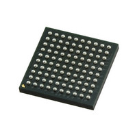
December 2007 Figure 35. 100_Ball LFBGA Package 115 M9999-121007-1.5 ...
Page 116
MICREL, INC. 2180 FORTUNE DRIVE SAN JOSE, CA 95131 USA TEL: +1 (408) 944-0800 The information furnished by Micrel in this data sheet is believed to be accurate and reliable. However, no responsibility is assumed by Micrel for its use. ...