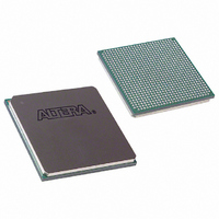
EP3SL150F780C2N Altera, EP3SL150F780C2N Datasheet - Page 25

EP3SL150F780C2N
Manufacturer Part Number
EP3SL150F780C2N
Description
IC STRATIX III FPGA 150K 780FBGA
Manufacturer
Altera
Series
Stratix® IIIr
Datasheets
1.EP3SL150F780C4N.pdf
(16 pages)
2.EP3SL150F780C4N.pdf
(332 pages)
3.EP3SL150F780C4N.pdf
(456 pages)
4.EP3SL150F780C2N.pdf
(341 pages)
Specifications of EP3SL150F780C2N
Number Of Logic Elements/cells
142500
Number Of Labs/clbs
5700
Total Ram Bits
6390
Number Of I /o
488
Voltage - Supply
0.86 V ~ 1.15 V
Mounting Type
Surface Mount
Operating Temperature
0°C ~ 85°C
Package / Case
780-FBGA
Family Name
Stratix III
Number Of Logic Blocks/elements
142500
# I/os (max)
488
Frequency (max)
600MHz
Process Technology
65nm
Operating Supply Voltage (typ)
1.1V
Logic Cells
142500
Ram Bits
6543360
Operating Supply Voltage (min)
1.05V
Operating Supply Voltage (max)
1.15V
Operating Temp Range
0C to 85C
Operating Temperature Classification
Commercial
Mounting
Surface Mount
Pin Count
780
Package Type
FC-FBGA
For Use With
544-2568 - KIT DEVELOPMENT STRATIX III
Lead Free Status / RoHS Status
Lead free / RoHS Compliant
Number Of Gates
-
Lead Free Status / Rohs Status
Compliant
Other names
544-2405
EP3SL150F780C2NES
EP3SL150F780C2NES
Available stocks
Company
Part Number
Manufacturer
Quantity
Price
Company:
Part Number:
EP3SL150F780C2N
Manufacturer:
ALTERA
Quantity:
200
Part Number:
EP3SL150F780C2N
Manufacturer:
ALTERA
Quantity:
20 000
- EP3SL150F780C4N PDF datasheet
- EP3SL150F780C4N PDF datasheet #2
- EP3SL150F780C4N PDF datasheet #3
- EP3SL150F780C2N PDF datasheet #4
- Current page: 25 of 332
- Download datasheet (4Mb)
Chapter 1: Stratix III Device Datasheet: DC and Switching Characteristics
Switching Characteristics
Figure 1–3. LVDS Soft-CDR/DPA Sinusiodal Jitter Tolerance Specification for Stratix III Devices
© July 2010 Altera Corporation
f
Figure 1–3
for Stratix III devices.
Table 1–27
devices.
Table 1–27. LVDS Soft-CDR/DPA Sinusoidal Jitter Mask Values for Stratix III Devices
External Memory Interface Specifications
The following sections describe the external memory I/O timing specifications and
the DLL and DQS block specifications.
For more information about the maximum clock rate support for external memory
interfaces with a half-rate or full-rate controller, refer to
Specifications
External Memory I/O Timing Specifications
Table 1–28
write data paths. Use these specifications to determine timing margins for source
synchronous paths between the Stratix III FPGA and the external memory device. For
more information, refer to the figure for “SW (sampling window)” in the
on page
F1
F2
F3
F4
1–326.
shows the LVDS Soft-CDR/ DPA sinusoidal jitter tolerance specifications
lists the LVDS Soft-CDR/ DPA sinusiodal jitter mask values for Stratix III
and
Jitter Frequency (Hz)
of the External Memory Interfaces Handbook.
Table 1–29
50,000,000
1,493,000
list Stratix III device timing uncertainties on the read and
10,000
17,565
Jitter Amplitude
25.000
25.000
0.350
0.350
Section III: System Performance
Stratix III Device Handbook, Volume 2
“Glossary”
Unit
UI
UI
UI
UI
1–25
Related parts for EP3SL150F780C2N
Image
Part Number
Description
Manufacturer
Datasheet
Request
R

Part Number:
Description:
CYCLONE II STARTER KIT EP2C20N
Manufacturer:
Altera
Datasheet:

Part Number:
Description:
CPLD, EP610 Family, ECMOS Process, 300 Gates, 16 Macro Cells, 16 Reg., 16 User I/Os, 5V Supply, 35 Speed Grade, 24DIP
Manufacturer:
Altera Corporation
Datasheet:

Part Number:
Description:
CPLD, EP610 Family, ECMOS Process, 300 Gates, 16 Macro Cells, 16 Reg., 16 User I/Os, 5V Supply, 15 Speed Grade, 24DIP
Manufacturer:
Altera Corporation
Datasheet:

Part Number:
Description:
Manufacturer:
Altera Corporation
Datasheet:

Part Number:
Description:
CPLD, EP610 Family, ECMOS Process, 300 Gates, 16 Macro Cells, 16 Reg., 16 User I/Os, 5V Supply, 30 Speed Grade, 24DIP
Manufacturer:
Altera Corporation
Datasheet:

Part Number:
Description:
High-performance, low-power erasable programmable logic devices with 8 macrocells, 10ns
Manufacturer:
Altera Corporation
Datasheet:

Part Number:
Description:
High-performance, low-power erasable programmable logic devices with 8 macrocells, 7ns
Manufacturer:
Altera Corporation
Datasheet:

Part Number:
Description:
Classic EPLD
Manufacturer:
Altera Corporation
Datasheet:

Part Number:
Description:
High-performance, low-power erasable programmable logic devices with 8 macrocells, 10ns
Manufacturer:
Altera Corporation
Datasheet:

Part Number:
Description:
Manufacturer:
Altera Corporation
Datasheet:

Part Number:
Description:
Manufacturer:
Altera Corporation
Datasheet:

Part Number:
Description:
Manufacturer:
Altera Corporation
Datasheet:

Part Number:
Description:
CPLD, EP610 Family, ECMOS Process, 300 Gates, 16 Macro Cells, 16 Reg., 16 User I/Os, 5V Supply, 25 Speed Grade, 24DIP
Manufacturer:
Altera Corporation
Datasheet:


