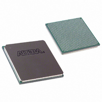
EP1S30F780I6N Altera, EP1S30F780I6N Datasheet - Page 39

EP1S30F780I6N
Manufacturer Part Number
EP1S30F780I6N
Description
IC STRATIX FPGA 30K LE 780-FBGA
Manufacturer
Altera
Series
Stratix®r
Datasheet
1.EP1S10F780C7.pdf
(276 pages)
Specifications of EP1S30F780I6N
Number Of Logic Elements/cells
32470
Number Of Labs/clbs
3247
Total Ram Bits
3317184
Number Of I /o
597
Voltage - Supply
1.425 V ~ 1.575 V
Mounting Type
Surface Mount
Operating Temperature
-40°C ~ 100°C
Package / Case
780-FBGA
Lead Free Status / RoHS Status
Lead free / RoHS Compliant
Number Of Gates
-
Available stocks
Company
Part Number
Manufacturer
Quantity
Price
Company:
Part Number:
EP1S30F780I6N
Manufacturer:
ALTERA
Quantity:
996
- Current page: 39 of 276
- Download datasheet (4Mb)
Altera Corporation
July 2005
Shift Register Support
You can configure embedded memory blocks to implement shift registers
for DSP applications such as pseudo-random number generators, multi-
channel filtering, auto-correlation, and cross-correlation functions. These
and other DSP applications require local data storage, traditionally
implemented with standard flip-flops, which can quickly consume many
logic cells and routing resources for large shift registers. A more efficient
alternative is to use embedded memory as a shift register block, which
saves logic cell and routing resources and provides a more efficient
implementation with the dedicated circuitry.
The size of a w × m × n shift register is determined by the input data
width (w), the length of the taps (m), and the number of taps (n). The size
of a w × m × n shift register must be less than or equal to the maximum
number of memory bits in the respective block: 576 bits for the M512
RAM block and 4,608 bits for the M4K RAM block. The total number of
shift register outputs (number of taps n × width w) must be less than the
maximum data width of the RAM block (18 for M512 blocks, 36 for M4K
blocks). To create larger shift registers, the memory blocks are cascaded
together.
Data is written into each address location at the falling edge of the clock
and read from the address at the rising edge of the clock. The shift register
mode logic automatically controls the positive and negative edge
clocking to shift the data in one clock cycle.
TriMatrix memory block in the shift register mode.
Stratix Device Handbook, Volume 1
Figure 2–14
Stratix Architecture
shows the
2–25
Related parts for EP1S30F780I6N
Image
Part Number
Description
Manufacturer
Datasheet
Request
R

Part Number:
Description:
CYCLONE II STARTER KIT EP2C20N
Manufacturer:
Altera
Datasheet:

Part Number:
Description:
CPLD, EP610 Family, ECMOS Process, 300 Gates, 16 Macro Cells, 16 Reg., 16 User I/Os, 5V Supply, 35 Speed Grade, 24DIP
Manufacturer:
Altera Corporation
Datasheet:

Part Number:
Description:
CPLD, EP610 Family, ECMOS Process, 300 Gates, 16 Macro Cells, 16 Reg., 16 User I/Os, 5V Supply, 15 Speed Grade, 24DIP
Manufacturer:
Altera Corporation
Datasheet:

Part Number:
Description:
Manufacturer:
Altera Corporation
Datasheet:

Part Number:
Description:
CPLD, EP610 Family, ECMOS Process, 300 Gates, 16 Macro Cells, 16 Reg., 16 User I/Os, 5V Supply, 30 Speed Grade, 24DIP
Manufacturer:
Altera Corporation
Datasheet:

Part Number:
Description:
High-performance, low-power erasable programmable logic devices with 8 macrocells, 10ns
Manufacturer:
Altera Corporation
Datasheet:

Part Number:
Description:
High-performance, low-power erasable programmable logic devices with 8 macrocells, 7ns
Manufacturer:
Altera Corporation
Datasheet:

Part Number:
Description:
Classic EPLD
Manufacturer:
Altera Corporation
Datasheet:

Part Number:
Description:
High-performance, low-power erasable programmable logic devices with 8 macrocells, 10ns
Manufacturer:
Altera Corporation
Datasheet:

Part Number:
Description:
Manufacturer:
Altera Corporation
Datasheet:

Part Number:
Description:
Manufacturer:
Altera Corporation
Datasheet:

Part Number:
Description:
Manufacturer:
Altera Corporation
Datasheet:

Part Number:
Description:
CPLD, EP610 Family, ECMOS Process, 300 Gates, 16 Macro Cells, 16 Reg., 16 User I/Os, 5V Supply, 25 Speed Grade, 24DIP
Manufacturer:
Altera Corporation
Datasheet:


