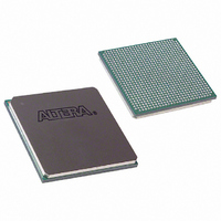
EP1S30F780I6N Altera, EP1S30F780I6N Datasheet - Page 174

EP1S30F780I6N
Manufacturer Part Number
EP1S30F780I6N
Description
IC STRATIX FPGA 30K LE 780-FBGA
Manufacturer
Altera
Series
Stratix®r
Datasheet
1.EP1S10F780C7.pdf
(276 pages)
Specifications of EP1S30F780I6N
Number Of Logic Elements/cells
32470
Number Of Labs/clbs
3247
Total Ram Bits
3317184
Number Of I /o
597
Voltage - Supply
1.425 V ~ 1.575 V
Mounting Type
Surface Mount
Operating Temperature
-40°C ~ 100°C
Package / Case
780-FBGA
Lead Free Status / RoHS Status
Lead free / RoHS Compliant
Number Of Gates
-
Available stocks
Company
Part Number
Manufacturer
Quantity
Price
Company:
Part Number:
EP1S30F780I6N
Manufacturer:
ALTERA
Quantity:
996
- Current page: 174 of 276
- Download datasheet (4Mb)
Operating Conditions
4–4
Stratix Device Handbook, Volume 1
Notes to
(1)
(2)
(3)
(4)
(5)
(6)
(7)
(8)
(9)
(10) Drive strength is programmable according to the values shown in the Stratix Architecture chapter of the Stratix
V
V
V
V
V
V
V
V
V
V
Table 4–7. 1.8-V I/O Specifications
Table 4–8. 1.5-V I/O Specifications
CCIO
I H
IL
OH
OL
CCIO
I H
IL
OH
OL
Symbol
Symbol
See the Operating Requirements for Altera Devices Data Sheet.
Conditions beyond those listed in
operation at the absolute maximum ratings for extended periods of time may have adverse affects on the device.
Minimum DC input is –0.5 V. During transitions, the inputs may undershoot to –2.0 V for input currents less than
100 mA and periods shorter than 20 ns, or overshoot to the voltage shown in
for input currents less than 100 mA. The overshoot is dependent upon duty cycle of the signal. The DC case is
equivalent to 100% duty cycle.
Maximum V
V
All pins, including dedicated inputs, clock, I/O, and JTAG pins, may be driven before V
powered.
Typical values are for T
This value is specified for normal device operation. The value may vary during power-up. This applies for all
V
Pin pull-up resistance values will lower if an external source drives the pin higher than V
Device Handbook, Volume 1.
CCIO
CCIO
Tables 4–1
maximum and minimum conditions for LVPECL, LVDS, and 3.3-V PCML are shown in parentheses.
settings (3.3, 2.5, 1.8, and 1.5 V).
Output supply voltage
High-level input voltage
Low-level input voltage
High-level output voltage
Low-level output voltage
Output supply voltage
High-level input voltage
Low-level input voltage
High-level output voltage
Low-level output voltage
CC
rise time is 100 ms, and V
through 4–8:
Parameter
Parameter
A
= 25°C, V
Table 4–9. Overshoot Input Voltage with Respect to Duty Cycle (Part 1 of 2)
Table 4–1
CCINT
= 1.5 V, and V
CC
must rise monotonically.
may cause permanent damage to a device. Additionally, device
Vin (V)
4.0
4.1
4.2
I
I
I
I
OH
OL
OH
OL
= 2 to 8 mA
= 2 mA
= –2 to –8 mA
= –2 mA
Conditions
Conditions
CCIO
= 1.5 V, 1.8 V, 2.5 V, and 3.3 V.
(10)
(10)
(10)
(10)
0.65 × V
0.65 × V
0.75 × V
V
Minimum
Minimum
CCIO
Table
1.65
–0.3
–0.3
Maximum Duty Cycle (%)
1.4
– 0.45
4–9, based on input duty cycle
CCIO
CCIO
CCIO
CCINT
0.35 × V
0.35 × V
0.25 × V
CCIO
V
Maximum
Maximum
100
90
50
CCIO
Altera Corporation
1.95
2.25
0.45
.
1.6
and V
+ 0.3
CCIO
CCIO
CCIO
January 2006
CCIO
are
Unit
Unit
V
V
V
V
V
V
V
V
V
V
Related parts for EP1S30F780I6N
Image
Part Number
Description
Manufacturer
Datasheet
Request
R

Part Number:
Description:
CYCLONE II STARTER KIT EP2C20N
Manufacturer:
Altera
Datasheet:

Part Number:
Description:
CPLD, EP610 Family, ECMOS Process, 300 Gates, 16 Macro Cells, 16 Reg., 16 User I/Os, 5V Supply, 35 Speed Grade, 24DIP
Manufacturer:
Altera Corporation
Datasheet:

Part Number:
Description:
CPLD, EP610 Family, ECMOS Process, 300 Gates, 16 Macro Cells, 16 Reg., 16 User I/Os, 5V Supply, 15 Speed Grade, 24DIP
Manufacturer:
Altera Corporation
Datasheet:

Part Number:
Description:
Manufacturer:
Altera Corporation
Datasheet:

Part Number:
Description:
CPLD, EP610 Family, ECMOS Process, 300 Gates, 16 Macro Cells, 16 Reg., 16 User I/Os, 5V Supply, 30 Speed Grade, 24DIP
Manufacturer:
Altera Corporation
Datasheet:

Part Number:
Description:
High-performance, low-power erasable programmable logic devices with 8 macrocells, 10ns
Manufacturer:
Altera Corporation
Datasheet:

Part Number:
Description:
High-performance, low-power erasable programmable logic devices with 8 macrocells, 7ns
Manufacturer:
Altera Corporation
Datasheet:

Part Number:
Description:
Classic EPLD
Manufacturer:
Altera Corporation
Datasheet:

Part Number:
Description:
High-performance, low-power erasable programmable logic devices with 8 macrocells, 10ns
Manufacturer:
Altera Corporation
Datasheet:

Part Number:
Description:
Manufacturer:
Altera Corporation
Datasheet:

Part Number:
Description:
Manufacturer:
Altera Corporation
Datasheet:

Part Number:
Description:
Manufacturer:
Altera Corporation
Datasheet:

Part Number:
Description:
CPLD, EP610 Family, ECMOS Process, 300 Gates, 16 Macro Cells, 16 Reg., 16 User I/Os, 5V Supply, 25 Speed Grade, 24DIP
Manufacturer:
Altera Corporation
Datasheet:


