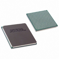
EP1S30F780I6N Altera, EP1S30F780I6N Datasheet - Page 155

EP1S30F780I6N
Manufacturer Part Number
EP1S30F780I6N
Description
IC STRATIX FPGA 30K LE 780-FBGA
Manufacturer
Altera
Series
Stratix®r
Datasheet
1.EP1S10F780C7.pdf
(276 pages)
Specifications of EP1S30F780I6N
Number Of Logic Elements/cells
32470
Number Of Labs/clbs
3247
Total Ram Bits
3317184
Number Of I /o
597
Voltage - Supply
1.425 V ~ 1.575 V
Mounting Type
Surface Mount
Operating Temperature
-40°C ~ 100°C
Package / Case
780-FBGA
Lead Free Status / RoHS Status
Lead free / RoHS Compliant
Number Of Gates
-
Available stocks
Company
Part Number
Manufacturer
Quantity
Price
Company:
Part Number:
EP1S30F780I6N
Manufacturer:
ALTERA
Quantity:
996
- Current page: 155 of 276
- Download datasheet (4Mb)
IEEE Std. 1149.1
(JTAG)
Boundary-Scan
Support
Altera Corporation
July 2005
S51003-1.3
All Stratix
IEEE Std. 1149.1a-1990 specification. JTAG boundary-scan testing can be
performed either before or after, but not during configuration. Stratix
devices can also use the JTAG port for configuration together with either
the Quartus
Byte-Code Files (.jbc).
Stratix devices support IOE I/O standard setting reconfiguration through
the JTAG BST chain. The JTAG chain can update the I/O standard for all
input and output pins any time before or during user mode through the
CONFIG_IO instruction. You can use this ability for JTAG testing before
configuration when some of the Stratix pins drive or receive from other
devices on the board using voltage-referenced standards. Since the Stratix
device may not be configured before JTAG testing, the I/O pins may not
be configured for appropriate electrical standards for chip-to-chip
communication. Programming those I/O standards via JTAG allows you
to fully test the I/O connection to other devices.
The enhanced PLL reconfiguration bits are part of the JTAG chain before
configuration and after power-up. After device configuration, the PLL
reconfiguration bits are not part of the JTAG chain.
The JTAG pins support 1.5-V/1.8-V or 2.5-V/3.3-V I/O standards. The
TDO pin voltage is determined by the V
The VCCSEL pin selects whether the JTAG inputs are 1.5-V, 1.8-V, 2.5-V, or
3.3-V compatible.
Stratix devices also use the JTAG port to monitor the logic operation of the
device with the SignalTap
support the JTAG instructions shown in
The Quartus II software has an Auto Usercode feature where you can
choose to use the checksum value of a programming file as the JTAG user
code. If selected, the checksum is automatically loaded to the USERCODE
register. In the Settings dialog box in the Assignments menu, click Device
& Pin Options, then General, and then turn on the Auto Usercode
option.
®
®
devices provide JTAG BST circuitry that complies with the
II software or hardware using either Jam Files (.jam) or Jam
3. Configuration & Testing
®
II embedded logic analyzer. Stratix devices
CCIO
Table
of the bank where it resides.
3–1.
3–1
Related parts for EP1S30F780I6N
Image
Part Number
Description
Manufacturer
Datasheet
Request
R

Part Number:
Description:
CYCLONE II STARTER KIT EP2C20N
Manufacturer:
Altera
Datasheet:

Part Number:
Description:
CPLD, EP610 Family, ECMOS Process, 300 Gates, 16 Macro Cells, 16 Reg., 16 User I/Os, 5V Supply, 35 Speed Grade, 24DIP
Manufacturer:
Altera Corporation
Datasheet:

Part Number:
Description:
CPLD, EP610 Family, ECMOS Process, 300 Gates, 16 Macro Cells, 16 Reg., 16 User I/Os, 5V Supply, 15 Speed Grade, 24DIP
Manufacturer:
Altera Corporation
Datasheet:

Part Number:
Description:
Manufacturer:
Altera Corporation
Datasheet:

Part Number:
Description:
CPLD, EP610 Family, ECMOS Process, 300 Gates, 16 Macro Cells, 16 Reg., 16 User I/Os, 5V Supply, 30 Speed Grade, 24DIP
Manufacturer:
Altera Corporation
Datasheet:

Part Number:
Description:
High-performance, low-power erasable programmable logic devices with 8 macrocells, 10ns
Manufacturer:
Altera Corporation
Datasheet:

Part Number:
Description:
High-performance, low-power erasable programmable logic devices with 8 macrocells, 7ns
Manufacturer:
Altera Corporation
Datasheet:

Part Number:
Description:
Classic EPLD
Manufacturer:
Altera Corporation
Datasheet:

Part Number:
Description:
High-performance, low-power erasable programmable logic devices with 8 macrocells, 10ns
Manufacturer:
Altera Corporation
Datasheet:

Part Number:
Description:
Manufacturer:
Altera Corporation
Datasheet:

Part Number:
Description:
Manufacturer:
Altera Corporation
Datasheet:

Part Number:
Description:
Manufacturer:
Altera Corporation
Datasheet:

Part Number:
Description:
CPLD, EP610 Family, ECMOS Process, 300 Gates, 16 Macro Cells, 16 Reg., 16 User I/Os, 5V Supply, 25 Speed Grade, 24DIP
Manufacturer:
Altera Corporation
Datasheet:


