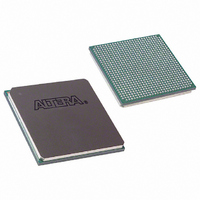
EP1S30F780I6N Altera, EP1S30F780I6N Datasheet - Page 141

EP1S30F780I6N
Manufacturer Part Number
EP1S30F780I6N
Description
IC STRATIX FPGA 30K LE 780-FBGA
Manufacturer
Altera
Series
Stratix®r
Datasheet
1.EP1S10F780C7.pdf
(276 pages)
Specifications of EP1S30F780I6N
Number Of Logic Elements/cells
32470
Number Of Labs/clbs
3247
Total Ram Bits
3317184
Number Of I /o
597
Voltage - Supply
1.425 V ~ 1.575 V
Mounting Type
Surface Mount
Operating Temperature
-40°C ~ 100°C
Package / Case
780-FBGA
Lead Free Status / RoHS Status
Lead free / RoHS Compliant
Number Of Gates
-
Available stocks
Company
Part Number
Manufacturer
Quantity
Price
Company:
Part Number:
EP1S30F780I6N
Manufacturer:
ALTERA
Quantity:
996
- Current page: 141 of 276
- Download datasheet (4Mb)
Altera Corporation
July 2005
SSTL-3 Class II
AGP (1× and 2× )
CTT
Table 2–32. I/O Support by Bank (Part 2 of 2)
I/O Standard
Each I/O bank has its own VCCIO pins. A single device can support 1.5-,
1.8-, 2.5-, and 3.3-V interfaces; each bank can support a different standard
independently. Each bank also has dedicated VREF pins to support any
one of the voltage-referenced standards (such as SSTL-3) independently.
Each I/O bank can support multiple standards with the same V
input and output pins. Each bank can support one voltage-referenced
I/O standard. For example, when V
LVTTL, LVCMOS, 3.3-V PCI, and SSTL-3 for inputs and outputs.
Differential On-Chip Termination
Stratix devices provide differential on-chip termination (LVDS I/O
standard) to reduce reflections and maintain signal integrity. Differential
on-chip termination simplifies board design by minimizing the number
of external termination resistors required. Termination can be placed
inside the package, eliminating small stubs that can still lead to
reflections. The internal termination is designed using transistors in the
linear region of operation.
Stratix devices support internal differential termination with a nominal
resistance value of 137.5 Ω for LVDS input receiver buffers. LVPECL
signals require an external termination resistor.
device with differential termination.
Top & Bottom Banks
(3, 4, 7 & 8)
v
v
v
Left & Right Banks
(1, 2, 5 & 6)
v
v
CCIO
Stratix Device Handbook, Volume 1
is 3.3 V, a bank can support
Figure 2–71
Enhanced PLL External
Clock Output Banks
(9, 10, 11 & 12)
Stratix Architecture
v
v
v
shows the
CCIO
2–127
for
Related parts for EP1S30F780I6N
Image
Part Number
Description
Manufacturer
Datasheet
Request
R

Part Number:
Description:
CYCLONE II STARTER KIT EP2C20N
Manufacturer:
Altera
Datasheet:

Part Number:
Description:
CPLD, EP610 Family, ECMOS Process, 300 Gates, 16 Macro Cells, 16 Reg., 16 User I/Os, 5V Supply, 35 Speed Grade, 24DIP
Manufacturer:
Altera Corporation
Datasheet:

Part Number:
Description:
CPLD, EP610 Family, ECMOS Process, 300 Gates, 16 Macro Cells, 16 Reg., 16 User I/Os, 5V Supply, 15 Speed Grade, 24DIP
Manufacturer:
Altera Corporation
Datasheet:

Part Number:
Description:
Manufacturer:
Altera Corporation
Datasheet:

Part Number:
Description:
CPLD, EP610 Family, ECMOS Process, 300 Gates, 16 Macro Cells, 16 Reg., 16 User I/Os, 5V Supply, 30 Speed Grade, 24DIP
Manufacturer:
Altera Corporation
Datasheet:

Part Number:
Description:
High-performance, low-power erasable programmable logic devices with 8 macrocells, 10ns
Manufacturer:
Altera Corporation
Datasheet:

Part Number:
Description:
High-performance, low-power erasable programmable logic devices with 8 macrocells, 7ns
Manufacturer:
Altera Corporation
Datasheet:

Part Number:
Description:
Classic EPLD
Manufacturer:
Altera Corporation
Datasheet:

Part Number:
Description:
High-performance, low-power erasable programmable logic devices with 8 macrocells, 10ns
Manufacturer:
Altera Corporation
Datasheet:

Part Number:
Description:
Manufacturer:
Altera Corporation
Datasheet:

Part Number:
Description:
Manufacturer:
Altera Corporation
Datasheet:

Part Number:
Description:
Manufacturer:
Altera Corporation
Datasheet:

Part Number:
Description:
CPLD, EP610 Family, ECMOS Process, 300 Gates, 16 Macro Cells, 16 Reg., 16 User I/Os, 5V Supply, 25 Speed Grade, 24DIP
Manufacturer:
Altera Corporation
Datasheet:


