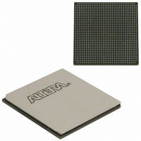
EP3SL150F1152C4N Altera, EP3SL150F1152C4N Datasheet - Page 98

EP3SL150F1152C4N
Manufacturer Part Number
EP3SL150F1152C4N
Description
IC STRATX III FPGA 150K 1152FBGA
Manufacturer
Altera
Series
Stratix® IIIr
Datasheets
1.EP3SL150F780C4N.pdf
(16 pages)
2.EP3SL150F780C4N.pdf
(332 pages)
3.EP3SL150F780C4N.pdf
(456 pages)
4.EP3SL150F1152C4N.pdf
(341 pages)
Specifications of EP3SL150F1152C4N
Number Of Logic Elements/cells
142500
Number Of Labs/clbs
5700
Total Ram Bits
6390
Number Of I /o
744
Voltage - Supply
0.86 V ~ 1.15 V
Mounting Type
Surface Mount
Operating Temperature
0°C ~ 85°C
Package / Case
1152-FBGA
Family Name
Stratix III
Number Of Logic Blocks/elements
142500
# I/os (max)
744
Frequency (max)
450MHz
Process Technology
65nm
Operating Supply Voltage (typ)
1.1V
Logic Cells
142500
Ram Bits
6543360
Operating Supply Voltage (min)
1.05V
Operating Supply Voltage (max)
1.15V
Operating Temp Range
0C to 85C
Operating Temperature Classification
Commercial
Mounting
Surface Mount
Pin Count
1152
Package Type
FC-FBGA
Operating Frequency Max
717MHz
Operating Temperature Range
0°C To +85°C
Logic Case Style
BGA
No. Of Pins
1152
Filter Terminals
SMD
Rohs Compliant
Yes
Core Supply Voltage
1.1V
For Use With
544-2568 - KIT DEVELOPMENT STRATIX III
Lead Free Status / RoHS Status
Lead free / RoHS Compliant
Number Of Gates
-
Lead Free Status / Rohs Status
Compliant
Other names
544-2407
EP3SL150F1152C4NES
EP3SL150F1152C4NES
Available stocks
Company
Part Number
Manufacturer
Quantity
Price
Company:
Part Number:
EP3SL150F1152C4N
Manufacturer:
ALTERA
Quantity:
3 000
Part Number:
EP3SL150F1152C4N
Manufacturer:
ALTERA
Quantity:
20 000
- EP3SL150F780C4N PDF datasheet
- EP3SL150F780C4N PDF datasheet #2
- EP3SL150F780C4N PDF datasheet #3
- EP3SL150F1152C4N PDF datasheet #4
- Current page: 98 of 456
- Download datasheet (7Mb)
4–18
Figure 4–17. Stratix III Shift-Register Memory Configuration
ROM Mode
FIFO Mode
Stratix III Device Handbook, Volume 1
f
1
w × m × n Shift Register
W
W
W
W
Figure 4–17
All Stratix III TriMatrix memory blocks support ROM mode. A .mif file initializes the
ROM content of these blocks. The address lines of the ROM are registered on M9K
and M144K blocks, but can be unregistered on MLABs. The outputs can be registered
or unregistered. Output registers can be asynchronously cleared. The ROM read
operation is identical to the read operation in the single-port RAM configuration.
All TriMatrix memory blocks support FIFO mode. MLABs are ideal for designs with
many small, shallow FIFO buffers. To implement FIFO buffers in your design, use the
Quartus II software FIFO MegaWizard Plug-In Manager. Both single and dual-clock
(asynchronous) FIFOs are supported.
For more information about implementing FIFO buffers, refer to the
Dual-Clock FIFO Megafunctions User
MLABs do not support mixed-width FIFO mode.
m-Bit Shift Register
m-Bit Shift Register
m-Bit Shift Register
m-Bit Shift Register
shows the TriMatrix memory block in shift-register mode.
Chapter 4: TriMatrix Embedded Memory Blocks in Stratix III Devices
Guide.
W
W
W
W
© May 2009 Altera Corporation
n Number of Taps
Single- and
Overview
Related parts for EP3SL150F1152C4N
Image
Part Number
Description
Manufacturer
Datasheet
Request
R

Part Number:
Description:
CYCLONE II STARTER KIT EP2C20N
Manufacturer:
Altera
Datasheet:

Part Number:
Description:
CPLD, EP610 Family, ECMOS Process, 300 Gates, 16 Macro Cells, 16 Reg., 16 User I/Os, 5V Supply, 35 Speed Grade, 24DIP
Manufacturer:
Altera Corporation
Datasheet:

Part Number:
Description:
CPLD, EP610 Family, ECMOS Process, 300 Gates, 16 Macro Cells, 16 Reg., 16 User I/Os, 5V Supply, 15 Speed Grade, 24DIP
Manufacturer:
Altera Corporation
Datasheet:

Part Number:
Description:
Manufacturer:
Altera Corporation
Datasheet:

Part Number:
Description:
CPLD, EP610 Family, ECMOS Process, 300 Gates, 16 Macro Cells, 16 Reg., 16 User I/Os, 5V Supply, 30 Speed Grade, 24DIP
Manufacturer:
Altera Corporation
Datasheet:

Part Number:
Description:
High-performance, low-power erasable programmable logic devices with 8 macrocells, 10ns
Manufacturer:
Altera Corporation
Datasheet:

Part Number:
Description:
High-performance, low-power erasable programmable logic devices with 8 macrocells, 7ns
Manufacturer:
Altera Corporation
Datasheet:

Part Number:
Description:
Classic EPLD
Manufacturer:
Altera Corporation
Datasheet:

Part Number:
Description:
High-performance, low-power erasable programmable logic devices with 8 macrocells, 10ns
Manufacturer:
Altera Corporation
Datasheet:

Part Number:
Description:
Manufacturer:
Altera Corporation
Datasheet:

Part Number:
Description:
Manufacturer:
Altera Corporation
Datasheet:

Part Number:
Description:
Manufacturer:
Altera Corporation
Datasheet:

Part Number:
Description:
CPLD, EP610 Family, ECMOS Process, 300 Gates, 16 Macro Cells, 16 Reg., 16 User I/Os, 5V Supply, 25 Speed Grade, 24DIP
Manufacturer:
Altera Corporation
Datasheet:


