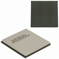
EP3SL150F1152C3N Altera, EP3SL150F1152C3N Datasheet - Page 416

EP3SL150F1152C3N
Manufacturer Part Number
EP3SL150F1152C3N
Description
IC STRATX III FPGA 150K 1152FBGA
Manufacturer
Altera
Series
Stratix® IIIr
Datasheets
1.EP3SL150F780C4N.pdf
(16 pages)
2.EP3SL150F780C4N.pdf
(332 pages)
3.EP3SL150F780C4N.pdf
(456 pages)
Specifications of EP3SL150F1152C3N
Number Of Logic Elements/cells
142500
Number Of Labs/clbs
5700
Total Ram Bits
6390
Number Of I /o
744
Voltage - Supply
0.86 V ~ 1.15 V
Mounting Type
Surface Mount
Operating Temperature
0°C ~ 85°C
Package / Case
1152-FBGA
For Use With
544-2568 - KIT DEVELOPMENT STRATIX III
Lead Free Status / RoHS Status
Lead free / RoHS Compliant
Number Of Gates
-
Other names
544-2408
EP3SL150F1152C3NES
EP3SL150F1152C3NES
Available stocks
Company
Part Number
Manufacturer
Quantity
Price
Company:
Part Number:
EP3SL150F1152C3N
Manufacturer:
ALTERA
Quantity:
490
- Current page: 416 of 456
- Download datasheet (7Mb)
13–18
IEEE Std. 1149.1 BST Circuitry
Stratix III Device Handbook, Volume 1
f
1
Figure 13–13. JTAG Chain of Mixed Voltages
Stratix III devices have dedicated JTAG pins and the IEEE Std. 1149.1 BST circuitry is
enabled upon device power-up. You can perform BST on Stratix III FPGAs before,
during, and after configuration. Stratix III FPGAs support the BYPASS, IDCODE, and
SAMPLE instructions during configuration without interrupting configuration. To
send all other JTAG instructions, you must interrupt configuration using the
CONFIG_IO instruction.
The CONFIG_IO instruction allows you to configure I/O buffers through the JTAG
port, and when issued, interrupts configuration. This instruction allows you to
perform board-level testing prior to configuring the Stratix III FPGA or you can wait
for the configuration device to complete configuration. After configuration is
interrupted and JTAG BST is complete, you must reconfigure the part through JTAG
(PULSE_CONFIG instruction) or by pulsing nCONFIG low.
When you perform JTAG boundary-scan testing before configuration, the nCONFIG
pin must be held low.
The chip-wide reset (DEV_CLRn) and chip-wide output enable (DEV_OE) pins on
Stratix III devices do not affect JTAG boundary-scan or configuration operations.
Toggling these pins does not disrupt BST operation (other than the expected BST
behavior).
When you design a board for JTAG configuration of Stratix III devices, you must
consider the connections for the dedicated configuration pins.
For more information about using the IEEE Std.1149.1 circuitry for device
configuration, refer to the
Stratix III Device Handbook.
Tester
Configuring Stratix III Devices
TDO
Chapter 13: IEEE 1149.1 (JTAG) Boundary-Scan Testing in Stratix III Devices
TDI
level accepted
Shift TDO to
by tester if
necessary.
Shifter
Level
V
3.3-V
CCIO
1.8-V tolerant.
Must be
V
1.5-V
CCIO
Must be 3.3-V tolerant.
V
2.5-V
CCIO
chapter in volume 1 of the
2.5-V tolerant.
Must be
V
1.8-V
CCIO
© July 2010 Altera Corporation
IEEE Std. 1149.1 BST Circuitry
Related parts for EP3SL150F1152C3N
Image
Part Number
Description
Manufacturer
Datasheet
Request
R

Part Number:
Description:
CYCLONE II STARTER KIT EP2C20N
Manufacturer:
Altera
Datasheet:

Part Number:
Description:
CPLD, EP610 Family, ECMOS Process, 300 Gates, 16 Macro Cells, 16 Reg., 16 User I/Os, 5V Supply, 35 Speed Grade, 24DIP
Manufacturer:
Altera Corporation
Datasheet:

Part Number:
Description:
CPLD, EP610 Family, ECMOS Process, 300 Gates, 16 Macro Cells, 16 Reg., 16 User I/Os, 5V Supply, 15 Speed Grade, 24DIP
Manufacturer:
Altera Corporation
Datasheet:

Part Number:
Description:
Manufacturer:
Altera Corporation
Datasheet:

Part Number:
Description:
CPLD, EP610 Family, ECMOS Process, 300 Gates, 16 Macro Cells, 16 Reg., 16 User I/Os, 5V Supply, 30 Speed Grade, 24DIP
Manufacturer:
Altera Corporation
Datasheet:

Part Number:
Description:
High-performance, low-power erasable programmable logic devices with 8 macrocells, 10ns
Manufacturer:
Altera Corporation
Datasheet:

Part Number:
Description:
High-performance, low-power erasable programmable logic devices with 8 macrocells, 7ns
Manufacturer:
Altera Corporation
Datasheet:

Part Number:
Description:
Classic EPLD
Manufacturer:
Altera Corporation
Datasheet:

Part Number:
Description:
High-performance, low-power erasable programmable logic devices with 8 macrocells, 10ns
Manufacturer:
Altera Corporation
Datasheet:

Part Number:
Description:
Manufacturer:
Altera Corporation
Datasheet:

Part Number:
Description:
Manufacturer:
Altera Corporation
Datasheet:

Part Number:
Description:
Manufacturer:
Altera Corporation
Datasheet:

Part Number:
Description:
CPLD, EP610 Family, ECMOS Process, 300 Gates, 16 Macro Cells, 16 Reg., 16 User I/Os, 5V Supply, 25 Speed Grade, 24DIP
Manufacturer:
Altera Corporation
Datasheet:


