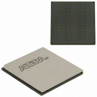
EP3SL150F1152C3N Altera, EP3SL150F1152C3N Datasheet - Page 411

EP3SL150F1152C3N
Manufacturer Part Number
EP3SL150F1152C3N
Description
IC STRATX III FPGA 150K 1152FBGA
Manufacturer
Altera
Series
Stratix® IIIr
Datasheets
1.EP3SL150F780C4N.pdf
(16 pages)
2.EP3SL150F780C4N.pdf
(332 pages)
3.EP3SL150F780C4N.pdf
(456 pages)
Specifications of EP3SL150F1152C3N
Number Of Logic Elements/cells
142500
Number Of Labs/clbs
5700
Total Ram Bits
6390
Number Of I /o
744
Voltage - Supply
0.86 V ~ 1.15 V
Mounting Type
Surface Mount
Operating Temperature
0°C ~ 85°C
Package / Case
1152-FBGA
For Use With
544-2568 - KIT DEVELOPMENT STRATIX III
Lead Free Status / RoHS Status
Lead free / RoHS Compliant
Number Of Gates
-
Other names
544-2408
EP3SL150F1152C3NES
EP3SL150F1152C3NES
Available stocks
Company
Part Number
Manufacturer
Quantity
Price
Company:
Part Number:
EP3SL150F1152C3N
Manufacturer:
ALTERA
Quantity:
490
- Current page: 411 of 456
- Download datasheet (7Mb)
Chapter 13: IEEE 1149.1 (JTAG) Boundary-Scan Testing in Stratix III Devices
IEEE Std. 1149.1 BST Operation Control
EXTEST Instruction Mode
Figure 13–10. IEEE Std. 1149.1 BST EXTEST Mode
© July 2010
Capture Phase
In the capture phase, the
signals at the pin, OEJ and
OUTJ, are loaded into the
capture registers. The CLOCK
signals are supplied by the TAP
controller's CLOCKDR output.
Previously retained data in the
update registers drive the
PIN_OUT, INJ, and allows the
I/O pin to tri-state or drive a
signal out.
A "1" in the OEJ update
register tri-states the output
buffer.
Shift and Update Phases
In the shift phase, the
previously captured signals at
the pin, OEJ and OUTJ, are
shifted out of the boundary-scan
register through the TDO pin using
CLOCK. As data is shifted out,
the patterns for the next test
can be shifted in through the
TDI pin.
In the update phase, data is
transferred from the capture
registers to the update
registers using the UPDATE
clock. The update registers
then drive the PIN_OUT, INJ,
and allow the I/O pin to
tri-state or drive a signal out.
Altera Corporation
Use the EXTEST instruction mode primarily to check external pin connections
between devices. Unlike the SAMPLE/PRELOAD mode, EXTEST allows test data to be
forced onto the pin signals. By forcing known logic high and low levels on output
pins, you can detect opens and shorts at pins of any device in the scan chain.
Figure 13–10
shows the capture, shift, and update phases of the EXTEST mode.
OUTJ
OUTJ
OEJ
OEJ
SDI
SDI
0
1
0
1
0
1
0
1
0
1
0
1
SHIFT
SHIFT
CLOCK
CLOCK
Registers
D
D
D
Registers
Capture
D
D
D
Capture
Q
Q
Q
Q
Q
Q
SDO
SDO
UPDATE
UPDATE
D
D
D
Registers
D
D
D
Registers
Update
Update
Q
Q
Q
Q
Q
Q
0
1
0
1
0
1
0
1
0
1
0
1
Stratix III Device Handbook, Volume 1
MODE
MODE
PIN_IN
PIN_IN
INJ
INJ
13–13
Related parts for EP3SL150F1152C3N
Image
Part Number
Description
Manufacturer
Datasheet
Request
R

Part Number:
Description:
CYCLONE II STARTER KIT EP2C20N
Manufacturer:
Altera
Datasheet:

Part Number:
Description:
CPLD, EP610 Family, ECMOS Process, 300 Gates, 16 Macro Cells, 16 Reg., 16 User I/Os, 5V Supply, 35 Speed Grade, 24DIP
Manufacturer:
Altera Corporation
Datasheet:

Part Number:
Description:
CPLD, EP610 Family, ECMOS Process, 300 Gates, 16 Macro Cells, 16 Reg., 16 User I/Os, 5V Supply, 15 Speed Grade, 24DIP
Manufacturer:
Altera Corporation
Datasheet:

Part Number:
Description:
Manufacturer:
Altera Corporation
Datasheet:

Part Number:
Description:
CPLD, EP610 Family, ECMOS Process, 300 Gates, 16 Macro Cells, 16 Reg., 16 User I/Os, 5V Supply, 30 Speed Grade, 24DIP
Manufacturer:
Altera Corporation
Datasheet:

Part Number:
Description:
High-performance, low-power erasable programmable logic devices with 8 macrocells, 10ns
Manufacturer:
Altera Corporation
Datasheet:

Part Number:
Description:
High-performance, low-power erasable programmable logic devices with 8 macrocells, 7ns
Manufacturer:
Altera Corporation
Datasheet:

Part Number:
Description:
Classic EPLD
Manufacturer:
Altera Corporation
Datasheet:

Part Number:
Description:
High-performance, low-power erasable programmable logic devices with 8 macrocells, 10ns
Manufacturer:
Altera Corporation
Datasheet:

Part Number:
Description:
Manufacturer:
Altera Corporation
Datasheet:

Part Number:
Description:
Manufacturer:
Altera Corporation
Datasheet:

Part Number:
Description:
Manufacturer:
Altera Corporation
Datasheet:

Part Number:
Description:
CPLD, EP610 Family, ECMOS Process, 300 Gates, 16 Macro Cells, 16 Reg., 16 User I/Os, 5V Supply, 25 Speed Grade, 24DIP
Manufacturer:
Altera Corporation
Datasheet:


