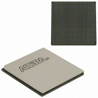
EP3SL150F1152C3N Altera, EP3SL150F1152C3N Datasheet - Page 405

EP3SL150F1152C3N
Manufacturer Part Number
EP3SL150F1152C3N
Description
IC STRATX III FPGA 150K 1152FBGA
Manufacturer
Altera
Series
Stratix® IIIr
Datasheets
1.EP3SL150F780C4N.pdf
(16 pages)
2.EP3SL150F780C4N.pdf
(332 pages)
3.EP3SL150F780C4N.pdf
(456 pages)
Specifications of EP3SL150F1152C3N
Number Of Logic Elements/cells
142500
Number Of Labs/clbs
5700
Total Ram Bits
6390
Number Of I /o
744
Voltage - Supply
0.86 V ~ 1.15 V
Mounting Type
Surface Mount
Operating Temperature
0°C ~ 85°C
Package / Case
1152-FBGA
For Use With
544-2568 - KIT DEVELOPMENT STRATIX III
Lead Free Status / RoHS Status
Lead free / RoHS Compliant
Number Of Gates
-
Other names
544-2408
EP3SL150F1152C3NES
EP3SL150F1152C3NES
Available stocks
Company
Part Number
Manufacturer
Quantity
Price
Company:
Part Number:
EP3SL150F1152C3N
Manufacturer:
ALTERA
Quantity:
490
- Current page: 405 of 456
- Download datasheet (7Mb)
Chapter 13: IEEE 1149.1 (JTAG) Boundary-Scan Testing in Stratix III Devices
IEEE Std. 1149.1 BST Operation Control
IEEE Std. 1149.1 BST Operation Control
Table 13–4. Stratix III JTAG Instructions
© July 2010
SAMPLE / PRELOAD
EXTEST
BYPASS
USERCODE
IDCODE
HIGHZ
CLAMP
ICR instructions
PULSE_NCONFIG
CONFIG_IO
Note to
(1) Bus hold and weak pull-up resistor features override the high-impedance state of the HIGHZ, CLAMP, and EXTEST instructions.
JTAG Instruction
Table
(1)
(1)
(1)
Altera Corporation
13–4:
Stratix III devices support the IEEE Std. 1149.1 (JTAG) instructions listed in
The IEEE Std. 1149.1 TAP controller, a 16-state machine clocked on the rising edge of
TCK, uses the TMS pin to control IEEE Std. 1149.1 operation in the device.
shows the TAP controller state machine.
00 0000 0101
00 0000 1111
11 1111 1111
00 0000 0111
00 0000 0110
00 0000 1011
00 0000 1010
00 0000 0001
00 0000 1101
Instruction
Code
—
Allows a snapshot of signals at the device pins to be captured and examined
during normal device operation, and permits an initial data pattern to be output at
the device pins. Also used by the SignalTap
Allows the external circuitry and board-level interconnects to be tested by forcing
a test pattern at the output pins and capturing test results at the input pins.
Places the 1-bit bypass register between the TDI and TDO pins, which allows
the BST data to pass synchronously through selected devices to adjacent devices
during normal device operation.
Places the 32-bit device identification register between TDI and TDO. The
USERCODE value are loaded into this Device ID register for shifting out through
TDO.
Selects the IDCODE register and places it between TDI and TDO, allowing the
IDCODE to be serially shifted out of TDO.
Places the 1-bit bypass register between the TDI and TDO pins, which allows
the BST data to pass synchronously through selected devices to adjacent devices
during normal device operation, while tri-stating all of the I/O pins.
Places the 1-bit bypass register between the TDI and TDO pins, which allows
the BST data to pass synchronously through selected devices to adjacent devices
during normal device operation while holding I/O pins to a state defined by the
data in the boundary-scan register.
Used when configuring a Stratix III device through the JTAG port with a
USB-Blaster™, ByteBlaster™ II, MasterBlaster™ or ByteBlasterMV™ download
cable, or when using a Jam File or Jam Byte-Code (JBC) File through an
embedded processor.
Emulates pulsing the nCONFIG pin low to trigger reconfiguration even though
the physical pin is unaffected.
Allows I/O reconfiguration through JTAG ports using the IOCSR for JTAG testing.
Can be executed before, after, or during configurations.
Description
®
II embedded logic analyzer.
Stratix III Device Handbook, Volume 1
Figure 13–5
Table
13–4.
13–7
Related parts for EP3SL150F1152C3N
Image
Part Number
Description
Manufacturer
Datasheet
Request
R

Part Number:
Description:
CYCLONE II STARTER KIT EP2C20N
Manufacturer:
Altera
Datasheet:

Part Number:
Description:
CPLD, EP610 Family, ECMOS Process, 300 Gates, 16 Macro Cells, 16 Reg., 16 User I/Os, 5V Supply, 35 Speed Grade, 24DIP
Manufacturer:
Altera Corporation
Datasheet:

Part Number:
Description:
CPLD, EP610 Family, ECMOS Process, 300 Gates, 16 Macro Cells, 16 Reg., 16 User I/Os, 5V Supply, 15 Speed Grade, 24DIP
Manufacturer:
Altera Corporation
Datasheet:

Part Number:
Description:
Manufacturer:
Altera Corporation
Datasheet:

Part Number:
Description:
CPLD, EP610 Family, ECMOS Process, 300 Gates, 16 Macro Cells, 16 Reg., 16 User I/Os, 5V Supply, 30 Speed Grade, 24DIP
Manufacturer:
Altera Corporation
Datasheet:

Part Number:
Description:
High-performance, low-power erasable programmable logic devices with 8 macrocells, 10ns
Manufacturer:
Altera Corporation
Datasheet:

Part Number:
Description:
High-performance, low-power erasable programmable logic devices with 8 macrocells, 7ns
Manufacturer:
Altera Corporation
Datasheet:

Part Number:
Description:
Classic EPLD
Manufacturer:
Altera Corporation
Datasheet:

Part Number:
Description:
High-performance, low-power erasable programmable logic devices with 8 macrocells, 10ns
Manufacturer:
Altera Corporation
Datasheet:

Part Number:
Description:
Manufacturer:
Altera Corporation
Datasheet:

Part Number:
Description:
Manufacturer:
Altera Corporation
Datasheet:

Part Number:
Description:
Manufacturer:
Altera Corporation
Datasheet:

Part Number:
Description:
CPLD, EP610 Family, ECMOS Process, 300 Gates, 16 Macro Cells, 16 Reg., 16 User I/Os, 5V Supply, 25 Speed Grade, 24DIP
Manufacturer:
Altera Corporation
Datasheet:


