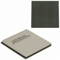
EP3SL150F1152C3N Altera, EP3SL150F1152C3N Datasheet - Page 364

EP3SL150F1152C3N
Manufacturer Part Number
EP3SL150F1152C3N
Description
IC STRATX III FPGA 150K 1152FBGA
Manufacturer
Altera
Series
Stratix® IIIr
Datasheets
1.EP3SL150F780C4N.pdf
(16 pages)
2.EP3SL150F780C4N.pdf
(332 pages)
3.EP3SL150F780C4N.pdf
(456 pages)
Specifications of EP3SL150F1152C3N
Number Of Logic Elements/cells
142500
Number Of Labs/clbs
5700
Total Ram Bits
6390
Number Of I /o
744
Voltage - Supply
0.86 V ~ 1.15 V
Mounting Type
Surface Mount
Operating Temperature
0°C ~ 85°C
Package / Case
1152-FBGA
For Use With
544-2568 - KIT DEVELOPMENT STRATIX III
Lead Free Status / RoHS Status
Lead free / RoHS Compliant
Number Of Gates
-
Other names
544-2408
EP3SL150F1152C3NES
EP3SL150F1152C3NES
Available stocks
Company
Part Number
Manufacturer
Quantity
Price
Company:
Part Number:
EP3SL150F1152C3N
Manufacturer:
ALTERA
Quantity:
490
- Current page: 364 of 456
- Download datasheet (7Mb)
11–32
Figure 11–16. PS Configuration Timing Waveform
Notes to
(1) The beginning of this waveform shows the device in user-mode. In user-mode, nCONFIG, nSTATUS, and CONF_DONE are at logic high levels.
(2) Upon power-up, the Stratix III device holds nSTATUS low for the time of the POR delay.
(3) Upon power-up, before and during configuration, CONF_DONE is low.
(4) Do not leave DCLK floating after configuration. You should drive it high or low, whichever is more convenient. DATA[0] is available as a user
(5) Two DCLK falling edges are required after CONF_DONE goes high to begin the initialization of the device.
Table 11–10. PS Timing Parameters for Stratix III Devices (Part 1 of 2)
Stratix III Device Handbook, Volume 1
t
t
t
t
t
t
t
t
t
t
t
t
f
t
Symbol
CF 2CD
CF 2ST0
CF G
STATUS
CF 2ST1
CF 2CK
ST2C K
DSU
DH
CH
CL
CLK
M AX
R
When nCONFIG is pulled low, a reconfiguration cycle begins.
I/O pin after configuration. The state of this pin depends on the dual-purpose pin settings.
Figure
nCONFIG low to CONF_DONE low
nCONFIG low to nSTATUS low
nCONFIG low pulse width
nSTATUS low pulse width
nCONFIG high to nSTATUS high
nCONFIG high to first rising edge on DCLK
nSTATUS high to first rising edge of DCLK
Data setup time before rising edge on DCLK
Data hold time after rising edge on DCLK
DCLK high time
DCLK low time
DCLK period
DCLK frequency
Input rise time
11–16:
CONF_DONE (3)
nSTATUS (2)
INIT_DONE
nCONFIG
PS Configuration Timing
Figure 11–16
device as an external host.
Table 11–10
User I/O
DCLK
DATA
t
CF2CD
t
CFG
Parameter
t
CF2ST1
defines the timing parameters for Stratix III devices for PS configuration.
t
CF2ST0
shows the timing waveform for PS configuration when using a MAX II
t
CF2CK
t
ST2CK
t
Bit 0 Bit 1 Bit 2 Bit 3
STATUS
High-Z
t
CH
t
CLK
t
DSU
t
CL
t
DH
(Note 1)
Bit n
(5)
Minimum
t
CD2UM
100
—
—
10
—
10
—
—
Chapter 11: Configuring Stratix III Devices
2
2
5
0
4
4
© March 2011 Altera Corporation
User Mode
(4)
(4)
Passive Serial Configuration
Maximum
100
100
800
800
100
—
—
—
—
—
—
—
—
40
(1)
(1)
Units
MHz
ns
ns
ns
ns
ns
ns
ns
ns
μs
μs
μs
μs
μs
Related parts for EP3SL150F1152C3N
Image
Part Number
Description
Manufacturer
Datasheet
Request
R

Part Number:
Description:
CYCLONE II STARTER KIT EP2C20N
Manufacturer:
Altera
Datasheet:

Part Number:
Description:
CPLD, EP610 Family, ECMOS Process, 300 Gates, 16 Macro Cells, 16 Reg., 16 User I/Os, 5V Supply, 35 Speed Grade, 24DIP
Manufacturer:
Altera Corporation
Datasheet:

Part Number:
Description:
CPLD, EP610 Family, ECMOS Process, 300 Gates, 16 Macro Cells, 16 Reg., 16 User I/Os, 5V Supply, 15 Speed Grade, 24DIP
Manufacturer:
Altera Corporation
Datasheet:

Part Number:
Description:
Manufacturer:
Altera Corporation
Datasheet:

Part Number:
Description:
CPLD, EP610 Family, ECMOS Process, 300 Gates, 16 Macro Cells, 16 Reg., 16 User I/Os, 5V Supply, 30 Speed Grade, 24DIP
Manufacturer:
Altera Corporation
Datasheet:

Part Number:
Description:
High-performance, low-power erasable programmable logic devices with 8 macrocells, 10ns
Manufacturer:
Altera Corporation
Datasheet:

Part Number:
Description:
High-performance, low-power erasable programmable logic devices with 8 macrocells, 7ns
Manufacturer:
Altera Corporation
Datasheet:

Part Number:
Description:
Classic EPLD
Manufacturer:
Altera Corporation
Datasheet:

Part Number:
Description:
High-performance, low-power erasable programmable logic devices with 8 macrocells, 10ns
Manufacturer:
Altera Corporation
Datasheet:

Part Number:
Description:
Manufacturer:
Altera Corporation
Datasheet:

Part Number:
Description:
Manufacturer:
Altera Corporation
Datasheet:

Part Number:
Description:
Manufacturer:
Altera Corporation
Datasheet:

Part Number:
Description:
CPLD, EP610 Family, ECMOS Process, 300 Gates, 16 Macro Cells, 16 Reg., 16 User I/Os, 5V Supply, 25 Speed Grade, 24DIP
Manufacturer:
Altera Corporation
Datasheet:


