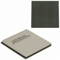
EP3SL150F1152C3N Altera, EP3SL150F1152C3N Datasheet - Page 339

EP3SL150F1152C3N
Manufacturer Part Number
EP3SL150F1152C3N
Description
IC STRATX III FPGA 150K 1152FBGA
Manufacturer
Altera
Series
Stratix® IIIr
Datasheets
1.EP3SL150F780C4N.pdf
(16 pages)
2.EP3SL150F780C4N.pdf
(332 pages)
3.EP3SL150F780C4N.pdf
(456 pages)
Specifications of EP3SL150F1152C3N
Number Of Logic Elements/cells
142500
Number Of Labs/clbs
5700
Total Ram Bits
6390
Number Of I /o
744
Voltage - Supply
0.86 V ~ 1.15 V
Mounting Type
Surface Mount
Operating Temperature
0°C ~ 85°C
Package / Case
1152-FBGA
For Use With
544-2568 - KIT DEVELOPMENT STRATIX III
Lead Free Status / RoHS Status
Lead free / RoHS Compliant
Number Of Gates
-
Other names
544-2408
EP3SL150F1152C3NES
EP3SL150F1152C3NES
Available stocks
Company
Part Number
Manufacturer
Quantity
Price
Company:
Part Number:
EP3SL150F1152C3N
Manufacturer:
ALTERA
Quantity:
490
- Current page: 339 of 456
- Download datasheet (7Mb)
Chapter 11: Configuring Stratix III Devices
Configuration Features
Remote System Upgrade
Power-On Reset Circuit
V
V
© March 2011 Altera Corporation
CCPGM
CCPD
Pins
Pins
f
f
1
Stratix III devices contain the remote update feature. For more information about this
feature, refer to the
Stratix III Device Handbook.
The POR circuit keeps the entire system in reset until the power supply voltage levels
have stabilized on power-up. On power-up, the device does not release nSTATUS
until V
power down, brown-out occurs if V
and V
In Stratix III devices, a pin-selectable option (PORSEL) is provided that allows you to
select a typical POR time setting of 12 ms or 100 ms. In both cases, you can extend the
POR time by using an external component to assert the nSTATUS pin low.
Stratix III devices offer a new power supply, V
pins and dual function pins. The configuration voltages supported are 1.8 V, 2.5 V,
3.0 V, and 3.3 V. Stratix III devices do not support the 1.5 V configuration.
Use this pin to power all dedicated configuration inputs, dedicated configuration
outputs, dedicated configuration bi-directional pins, and some of the dual functional
pins that you use for configuration. With V
have to share power lines with the regular I/O buffer in Stratix III devices.
The operating voltage for the configuration input pin is independent of the I/O
bank’s power supply V
voltage constraints on V
Stratix III devices have a dedicated programming power supply, V
connected to 3.3 V/3.0 V/2.5 V to power the I/O pre-drivers, the JTAG input and
output pins (TCK, TMS, TDI, TDO, and TRST), and the design security circuitry.
V
these supplies are not ramped up within this specified time, your Stratix III device
will not configure successfully. If your system does not allow ramp-up time of 100 ms
or less, you must hold nCONFIG low until all power supplies are stable.
For more information about the configuration pins power supply, refer to
Configuration Pins” on page
CCPGM
CC
CCPT
and V
, V
, V
CCPD
CCL
CCPD
, or V
, V
must ramp up from 0 V to the desired voltage level within 100 ms. If
CC
Remote System Upgrades with Stratix III Devices
CCPGM
, V
CCPD
CCIO
CCIO
drops below the threshold voltage.
, and V
during the configuration. Therefore, no configuration
are needed in Stratix III devices.
11–43.
CCPGM
CC
or V
are above the device’s POR trip point. On
CCL
CCPGM
ramps down below the POR trip point
CCPGM
, configuration input buffers do not
, for all the dedicated configuration
Stratix III Device Handbook, Volume 1
in volume 1 of the
CCPD
, which must be
“Device
11–7
Related parts for EP3SL150F1152C3N
Image
Part Number
Description
Manufacturer
Datasheet
Request
R

Part Number:
Description:
CYCLONE II STARTER KIT EP2C20N
Manufacturer:
Altera
Datasheet:

Part Number:
Description:
CPLD, EP610 Family, ECMOS Process, 300 Gates, 16 Macro Cells, 16 Reg., 16 User I/Os, 5V Supply, 35 Speed Grade, 24DIP
Manufacturer:
Altera Corporation
Datasheet:

Part Number:
Description:
CPLD, EP610 Family, ECMOS Process, 300 Gates, 16 Macro Cells, 16 Reg., 16 User I/Os, 5V Supply, 15 Speed Grade, 24DIP
Manufacturer:
Altera Corporation
Datasheet:

Part Number:
Description:
Manufacturer:
Altera Corporation
Datasheet:

Part Number:
Description:
CPLD, EP610 Family, ECMOS Process, 300 Gates, 16 Macro Cells, 16 Reg., 16 User I/Os, 5V Supply, 30 Speed Grade, 24DIP
Manufacturer:
Altera Corporation
Datasheet:

Part Number:
Description:
High-performance, low-power erasable programmable logic devices with 8 macrocells, 10ns
Manufacturer:
Altera Corporation
Datasheet:

Part Number:
Description:
High-performance, low-power erasable programmable logic devices with 8 macrocells, 7ns
Manufacturer:
Altera Corporation
Datasheet:

Part Number:
Description:
Classic EPLD
Manufacturer:
Altera Corporation
Datasheet:

Part Number:
Description:
High-performance, low-power erasable programmable logic devices with 8 macrocells, 10ns
Manufacturer:
Altera Corporation
Datasheet:

Part Number:
Description:
Manufacturer:
Altera Corporation
Datasheet:

Part Number:
Description:
Manufacturer:
Altera Corporation
Datasheet:

Part Number:
Description:
Manufacturer:
Altera Corporation
Datasheet:

Part Number:
Description:
CPLD, EP610 Family, ECMOS Process, 300 Gates, 16 Macro Cells, 16 Reg., 16 User I/Os, 5V Supply, 25 Speed Grade, 24DIP
Manufacturer:
Altera Corporation
Datasheet:


