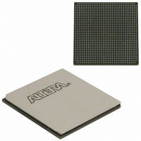
EP3SL150F1152C3N Altera, EP3SL150F1152C3N Datasheet - Page 302

EP3SL150F1152C3N
Manufacturer Part Number
EP3SL150F1152C3N
Description
IC STRATX III FPGA 150K 1152FBGA
Manufacturer
Altera
Series
Stratix® IIIr
Datasheets
1.EP3SL150F780C4N.pdf
(16 pages)
2.EP3SL150F780C4N.pdf
(332 pages)
3.EP3SL150F780C4N.pdf
(456 pages)
Specifications of EP3SL150F1152C3N
Number Of Logic Elements/cells
142500
Number Of Labs/clbs
5700
Total Ram Bits
6390
Number Of I /o
744
Voltage - Supply
0.86 V ~ 1.15 V
Mounting Type
Surface Mount
Operating Temperature
0°C ~ 85°C
Package / Case
1152-FBGA
For Use With
544-2568 - KIT DEVELOPMENT STRATIX III
Lead Free Status / RoHS Status
Lead free / RoHS Compliant
Number Of Gates
-
Other names
544-2408
EP3SL150F1152C3NES
EP3SL150F1152C3NES
Available stocks
Company
Part Number
Manufacturer
Quantity
Price
Company:
Part Number:
EP3SL150F1152C3N
Manufacturer:
ALTERA
Quantity:
490
- Current page: 302 of 456
- Download datasheet (7Mb)
9–8
Dynamic Phase Aligner (DPA)
Stratix III Device Handbook, Volume 1
Figure 9–7
deserialization factor set to 4.
Figure 9–7. Data Realignment Timing
The data realignment circuit can have up to 11 bit-times of insertion before a rollover
occurs. The programmable bit rollover point can be from 1 to 11 bit-times,
independent of the deserialization factor. An optional status port, RX_CDA_MAX, is
available to the FPGA from each channel to indicate when the preset rollover point is
reached.
The DPA block takes in high-speed serial data from the differential input buffer and
selects one of the eight phase clocks from the left/right PLL to sample the data. The
DPA chooses the phase closest to the phase of the serial data. The maximum phase
offset between the received data and the selected phase is 1/8 UI, which is the
maximum quantization error of the DPA. The eight phases of the clock are equally
divided, giving a 45° resolution.
Figure 9–8
incoming serial data.
Figure 9–8. DPA Clock Phase-to-Serial Data Timing Relationship
The DPA block continuously monitors the phase of the incoming serial data and
selects a new clock phase if required. You can prevent the DPA from selecting a new
clock phase by asserting the optional RX_DPLL_HOLD port, which is available for each
channel.
rx_channel_data_align
shows receiver output (RX_OUT) after one bit slip pulse with the
shows the possible phase relationships between the DPA clocks and the
rx_in
135˚
180˚
225˚
270˚
315˚
45˚
90˚
0˚
rx_outclock
0.125T
rx_out
rx_in
inclk
D0
vco
Chapter 9: High-Speed Differential I/O Interfaces and DPA in Stratix III Devices
3
D1
2
3210
1
T
D2
vco
0
3
D3
2
321x
1
D4
0
3
© July 2010 Altera Corporation
2
Dn
xx21
1
0
Differential Receiver
0321
Related parts for EP3SL150F1152C3N
Image
Part Number
Description
Manufacturer
Datasheet
Request
R

Part Number:
Description:
CYCLONE II STARTER KIT EP2C20N
Manufacturer:
Altera
Datasheet:

Part Number:
Description:
CPLD, EP610 Family, ECMOS Process, 300 Gates, 16 Macro Cells, 16 Reg., 16 User I/Os, 5V Supply, 35 Speed Grade, 24DIP
Manufacturer:
Altera Corporation
Datasheet:

Part Number:
Description:
CPLD, EP610 Family, ECMOS Process, 300 Gates, 16 Macro Cells, 16 Reg., 16 User I/Os, 5V Supply, 15 Speed Grade, 24DIP
Manufacturer:
Altera Corporation
Datasheet:

Part Number:
Description:
Manufacturer:
Altera Corporation
Datasheet:

Part Number:
Description:
CPLD, EP610 Family, ECMOS Process, 300 Gates, 16 Macro Cells, 16 Reg., 16 User I/Os, 5V Supply, 30 Speed Grade, 24DIP
Manufacturer:
Altera Corporation
Datasheet:

Part Number:
Description:
High-performance, low-power erasable programmable logic devices with 8 macrocells, 10ns
Manufacturer:
Altera Corporation
Datasheet:

Part Number:
Description:
High-performance, low-power erasable programmable logic devices with 8 macrocells, 7ns
Manufacturer:
Altera Corporation
Datasheet:

Part Number:
Description:
Classic EPLD
Manufacturer:
Altera Corporation
Datasheet:

Part Number:
Description:
High-performance, low-power erasable programmable logic devices with 8 macrocells, 10ns
Manufacturer:
Altera Corporation
Datasheet:

Part Number:
Description:
Manufacturer:
Altera Corporation
Datasheet:

Part Number:
Description:
Manufacturer:
Altera Corporation
Datasheet:

Part Number:
Description:
Manufacturer:
Altera Corporation
Datasheet:

Part Number:
Description:
CPLD, EP610 Family, ECMOS Process, 300 Gates, 16 Macro Cells, 16 Reg., 16 User I/Os, 5V Supply, 25 Speed Grade, 24DIP
Manufacturer:
Altera Corporation
Datasheet:


