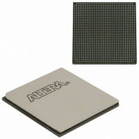
EP3SL150F1152C3N Altera, EP3SL150F1152C3N Datasheet - Page 301

EP3SL150F1152C3N
Manufacturer Part Number
EP3SL150F1152C3N
Description
IC STRATX III FPGA 150K 1152FBGA
Manufacturer
Altera
Series
Stratix® IIIr
Datasheets
1.EP3SL150F780C4N.pdf
(16 pages)
2.EP3SL150F780C4N.pdf
(332 pages)
3.EP3SL150F780C4N.pdf
(456 pages)
Specifications of EP3SL150F1152C3N
Number Of Logic Elements/cells
142500
Number Of Labs/clbs
5700
Total Ram Bits
6390
Number Of I /o
744
Voltage - Supply
0.86 V ~ 1.15 V
Mounting Type
Surface Mount
Operating Temperature
0°C ~ 85°C
Package / Case
1152-FBGA
For Use With
544-2568 - KIT DEVELOPMENT STRATIX III
Lead Free Status / RoHS Status
Lead free / RoHS Compliant
Number Of Gates
-
Other names
544-2408
EP3SL150F1152C3NES
EP3SL150F1152C3NES
Available stocks
Company
Part Number
Manufacturer
Quantity
Price
Company:
Part Number:
EP3SL150F1152C3N
Manufacturer:
ALTERA
Quantity:
490
- Current page: 301 of 456
- Download datasheet (7Mb)
Chapter 9: High-Speed Differential I/O Interfaces and DPA in Stratix III Devices
Differential Receiver
Figure 9–5. Receiver Block Diagram for Stratix III Devices
Figure 9–6. Deserializer Bypass for Stratix III Devices
Receiver Data Realignment Circuit (Bit Slip)
© July 2010
Altera Corporation
Up to 1.6 Gbps
Eight Phase Clocks
Figure 9–6
Skew in the transmitted data along with skew added by the link causes
channel-to-channel skew on the received serial data streams. If DPA is enabled, the
received data is captured with different clock phases on each channel. This may cause
the received data to be misaligned from channel to channel. To compensate for this
channel-to-channel skew and establish the correct received word boundary at each
channel, each receiver channel has a dedicated data realignment circuit that realigns
the data by inserting bit latencies into the serial stream.
An optional RX_CHANNEL_DATA_ALIGN port controls the bit insertion of each
receiver independently controlled from the internal logic. The data slips one bit for
every pulse on the RX_CHANNEL_DATA_ALIGN. The following are requirements for
the RX_CHANNEL_DATA_ALIGN signal:
■
■
■
■
rx_inclk
The minimum pulse width is one period of the parallel clock in the logic array
The minimum low time between pulses is one period of parallel clock
There is no maximum high or low time
Valid data is available two parallel clock cycles after the rising edge of
RX_CHANNEL_DATA_ALIGN
rx_in
+
–
shows the deseralizer bypass data path.
data
PLL _Lx /
PLL_Rx
DPA
8
retimed_
DPA_clk
data
diffioclk
load_en
Circuitry
DPA
Synchronizer
D
DPA Bypass Multiplexer
Q
Deserializer
IOE Supports SDR, DDR, or
Non-Registered Data Path
IOE
Realignment
Circuitry
Data
True
Receiver
Interface
PLD Logic
Array
Stratix III Device Handbook, Volume 1
Regional or
Global Clock
10
Internal
Logic
9–7
Related parts for EP3SL150F1152C3N
Image
Part Number
Description
Manufacturer
Datasheet
Request
R

Part Number:
Description:
CYCLONE II STARTER KIT EP2C20N
Manufacturer:
Altera
Datasheet:

Part Number:
Description:
CPLD, EP610 Family, ECMOS Process, 300 Gates, 16 Macro Cells, 16 Reg., 16 User I/Os, 5V Supply, 35 Speed Grade, 24DIP
Manufacturer:
Altera Corporation
Datasheet:

Part Number:
Description:
CPLD, EP610 Family, ECMOS Process, 300 Gates, 16 Macro Cells, 16 Reg., 16 User I/Os, 5V Supply, 15 Speed Grade, 24DIP
Manufacturer:
Altera Corporation
Datasheet:

Part Number:
Description:
Manufacturer:
Altera Corporation
Datasheet:

Part Number:
Description:
CPLD, EP610 Family, ECMOS Process, 300 Gates, 16 Macro Cells, 16 Reg., 16 User I/Os, 5V Supply, 30 Speed Grade, 24DIP
Manufacturer:
Altera Corporation
Datasheet:

Part Number:
Description:
High-performance, low-power erasable programmable logic devices with 8 macrocells, 10ns
Manufacturer:
Altera Corporation
Datasheet:

Part Number:
Description:
High-performance, low-power erasable programmable logic devices with 8 macrocells, 7ns
Manufacturer:
Altera Corporation
Datasheet:

Part Number:
Description:
Classic EPLD
Manufacturer:
Altera Corporation
Datasheet:

Part Number:
Description:
High-performance, low-power erasable programmable logic devices with 8 macrocells, 10ns
Manufacturer:
Altera Corporation
Datasheet:

Part Number:
Description:
Manufacturer:
Altera Corporation
Datasheet:

Part Number:
Description:
Manufacturer:
Altera Corporation
Datasheet:

Part Number:
Description:
Manufacturer:
Altera Corporation
Datasheet:

Part Number:
Description:
CPLD, EP610 Family, ECMOS Process, 300 Gates, 16 Macro Cells, 16 Reg., 16 User I/Os, 5V Supply, 25 Speed Grade, 24DIP
Manufacturer:
Altera Corporation
Datasheet:


