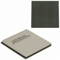
EP3SL150F1152C3N Altera, EP3SL150F1152C3N Datasheet - Page 281

EP3SL150F1152C3N
Manufacturer Part Number
EP3SL150F1152C3N
Description
IC STRATX III FPGA 150K 1152FBGA
Manufacturer
Altera
Series
Stratix® IIIr
Datasheets
1.EP3SL150F780C4N.pdf
(16 pages)
2.EP3SL150F780C4N.pdf
(332 pages)
3.EP3SL150F780C4N.pdf
(456 pages)
Specifications of EP3SL150F1152C3N
Number Of Logic Elements/cells
142500
Number Of Labs/clbs
5700
Total Ram Bits
6390
Number Of I /o
744
Voltage - Supply
0.86 V ~ 1.15 V
Mounting Type
Surface Mount
Operating Temperature
0°C ~ 85°C
Package / Case
1152-FBGA
For Use With
544-2568 - KIT DEVELOPMENT STRATIX III
Lead Free Status / RoHS Status
Lead free / RoHS Compliant
Number Of Gates
-
Other names
544-2408
EP3SL150F1152C3NES
EP3SL150F1152C3NES
Available stocks
Company
Part Number
Manufacturer
Quantity
Price
Company:
Part Number:
EP3SL150F1152C3N
Manufacturer:
ALTERA
Quantity:
490
- Current page: 281 of 456
- Download datasheet (7Mb)
Chapter 8: External Memory Interfaces in Stratix III Devices
Stratix III External Memory Interface Features
Figure 8–18. Stratix III Read Leveling Delay Chains and Multiplexers
Note to
(1) There is only one leveling delay chain per I/O bank with the same I/O number (for example, I/O banks 1A, 1B, and 1C). You can only have one
Dynamic OCT Control
© March 2010 Altera Corporation
memory controller in these I/O banks when you use leveling delay chains.
Figure
8–18:
f
f
1
Resynchronization
DQS
clock
Figure 8–18
The –90° write clock of the ALTMEMPHY megafunction feeds the write-leveling
circuitry to produce the clock that generates the DQS and DQ signals. During
initialization, the ALTMEMPHY megafunction picks the correct write-leveled clock
for the DQS and DQ clocks for each DQS/DQ group after sweeping all the available
clocks in the write calibration process. The DQ clock output is –90° phase-shifted
compared to the DQS clock output.
Similarly, the resynchronization clock feeds the read-leveling circuitry to produce the
optimal resynchronization and postamble clock for each DQS/DQ group in the
calibration process. Resynchronization and the postamble clocks can use different
clock outputs from the leveling circuitry. Output from the read-leveling circuitry can
also generate the half-rate resynchronization clock that goes to the FPGA fabric.
The ALTMEMPHY megafunction calibrates the alignment for read and write leveling
dynamically during the initialization process.
For more information about the ALTMEMPHY megafunction, refer to the
Implementing Altera Memory Interface
Figure 8–19
required to dynamically turn on OCT R
write.
For more information about dynamic OCT control, refer to the
Features
chapter.
shows the dynamic OCT control block. The block includes all the registers
illustrates the Stratix III read leveling circuitry.
Read-Leveled Resynchronization Clock
IP.
I/O Clock
T
(Note 1)
Divider
during a read and turn OCT R
Half-Rate Resynchronization Clock
Half-Rate Source
Synchronous Clock
Stratix III Device Handbook, Volume 1
Stratix III Device I/O
T
off during a
Volume 3:
8–33
Related parts for EP3SL150F1152C3N
Image
Part Number
Description
Manufacturer
Datasheet
Request
R

Part Number:
Description:
CYCLONE II STARTER KIT EP2C20N
Manufacturer:
Altera
Datasheet:

Part Number:
Description:
CPLD, EP610 Family, ECMOS Process, 300 Gates, 16 Macro Cells, 16 Reg., 16 User I/Os, 5V Supply, 35 Speed Grade, 24DIP
Manufacturer:
Altera Corporation
Datasheet:

Part Number:
Description:
CPLD, EP610 Family, ECMOS Process, 300 Gates, 16 Macro Cells, 16 Reg., 16 User I/Os, 5V Supply, 15 Speed Grade, 24DIP
Manufacturer:
Altera Corporation
Datasheet:

Part Number:
Description:
Manufacturer:
Altera Corporation
Datasheet:

Part Number:
Description:
CPLD, EP610 Family, ECMOS Process, 300 Gates, 16 Macro Cells, 16 Reg., 16 User I/Os, 5V Supply, 30 Speed Grade, 24DIP
Manufacturer:
Altera Corporation
Datasheet:

Part Number:
Description:
High-performance, low-power erasable programmable logic devices with 8 macrocells, 10ns
Manufacturer:
Altera Corporation
Datasheet:

Part Number:
Description:
High-performance, low-power erasable programmable logic devices with 8 macrocells, 7ns
Manufacturer:
Altera Corporation
Datasheet:

Part Number:
Description:
Classic EPLD
Manufacturer:
Altera Corporation
Datasheet:

Part Number:
Description:
High-performance, low-power erasable programmable logic devices with 8 macrocells, 10ns
Manufacturer:
Altera Corporation
Datasheet:

Part Number:
Description:
Manufacturer:
Altera Corporation
Datasheet:

Part Number:
Description:
Manufacturer:
Altera Corporation
Datasheet:

Part Number:
Description:
Manufacturer:
Altera Corporation
Datasheet:

Part Number:
Description:
CPLD, EP610 Family, ECMOS Process, 300 Gates, 16 Macro Cells, 16 Reg., 16 User I/Os, 5V Supply, 25 Speed Grade, 24DIP
Manufacturer:
Altera Corporation
Datasheet:


