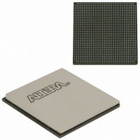
EP3SL150F1152C3N Altera, EP3SL150F1152C3N Datasheet - Page 275

EP3SL150F1152C3N
Manufacturer Part Number
EP3SL150F1152C3N
Description
IC STRATX III FPGA 150K 1152FBGA
Manufacturer
Altera
Series
Stratix® IIIr
Datasheets
1.EP3SL150F780C4N.pdf
(16 pages)
2.EP3SL150F780C4N.pdf
(332 pages)
3.EP3SL150F780C4N.pdf
(456 pages)
Specifications of EP3SL150F1152C3N
Number Of Logic Elements/cells
142500
Number Of Labs/clbs
5700
Total Ram Bits
6390
Number Of I /o
744
Voltage - Supply
0.86 V ~ 1.15 V
Mounting Type
Surface Mount
Operating Temperature
0°C ~ 85°C
Package / Case
1152-FBGA
For Use With
544-2568 - KIT DEVELOPMENT STRATIX III
Lead Free Status / RoHS Status
Lead free / RoHS Compliant
Number Of Gates
-
Other names
544-2408
EP3SL150F1152C3NES
EP3SL150F1152C3NES
Available stocks
Company
Part Number
Manufacturer
Quantity
Price
Company:
Part Number:
EP3SL150F1152C3N
Manufacturer:
ALTERA
Quantity:
490
- Current page: 275 of 456
- Download datasheet (7Mb)
Chapter 8: External Memory Interfaces in Stratix III Devices
Stratix III External Memory Interface Features
© March 2010 Altera Corporation
f
For the frequency range of each mode, refer to the
Stratix III Devices
Table 8–10. Stratix III DLL Frequency Modes
For 0° shift, the DQS signal bypasses both the DLL and DQS logic blocks. The
Quartus II software automatically sets DQ input delay chains so that the skew
between the DQ and DQS pin at the DQ IOE registers is negligible when the 0° shift is
implemented. You can feed the DQS delay settings to the DQS logic block and logic
array.
The shifted DQS signal goes to the DQS bus to clock the IOE input registers of the DQ
pins. The signal can also go into the logic array for resynchronization if you are not
using the IOE resynchronization registers. The shifted CQn signal can only go to the
negative-edge input register in the DQ IOE and is only used for QDR II+ and
QDR II SRAM interfaces.
Phase Offset Control
Each DLL has two phase-offset modules and can provide two separate DQS delay
settings with independent offset, one for the top and bottom I/O bank and one for the
left and right I/O bank, so you can fine-tune the DQS phase shift settings between
two different sides of the device. Even though you have independent phase offset
control, the frequency of the interface using the same DLL has to be the same. Use the
phase offset control module for making small shifts to the input signal; Use the DQS
phase-shift circuitry for larger signal shifts. For example, if the DLL only offers a
multiple of 30° phase shift, but your interface requires a 67.5° phase shift on the DQS
signal, you can use two delay chains in the DQS logic blocks to give you 60° phase
shift and use the phase offset control feature to implement the extra 7.5° phase shift.
You can either use a static phase offset or a dynamic phase offset to implement the
additional phase shift. The available additional phase shift is implemented in
2’s-complement in Gray-code between settings –64 to +63 for frequency modes 0, 1, 2,
and 3, and between settings –32 to +31 for frequency modes 4, 5, and 6. An additional
bit indicates whether the setting has a positive or negative value. The DQS phase shift
is the sum of the DLL delay settings and the user selected phase offset settings. The
maximum is setting 64 for frequency modes 0, 1, 2, and 3, and setting 32 for frequency
modes 4, 5, 6, and 7 so the actual physical offset setting range is 64 or 32 subtracted by
the DQS delay settings from the DLL.
Frequency Mode
0
1
2
3
4
5
6
7
chapter.
Available Phase Shift
22.5°, 45°, 67.5°, 90°
60°, 120°, 180°, 240°
36°, 72°, 108°, 144°
45°, 90°, 135°, 180°
36°, 72°, 108°, 144°
45°, 90°, 135°, 180°
30°, 60°, 90°, 120°
30°, 60°, 90°, 120°
DC and Switching Characteristics of
Stratix III Device Handbook, Volume 1
Number of Delay Chains
16
12
10
12
10
8
8
6
8–27
Related parts for EP3SL150F1152C3N
Image
Part Number
Description
Manufacturer
Datasheet
Request
R

Part Number:
Description:
CYCLONE II STARTER KIT EP2C20N
Manufacturer:
Altera
Datasheet:

Part Number:
Description:
CPLD, EP610 Family, ECMOS Process, 300 Gates, 16 Macro Cells, 16 Reg., 16 User I/Os, 5V Supply, 35 Speed Grade, 24DIP
Manufacturer:
Altera Corporation
Datasheet:

Part Number:
Description:
CPLD, EP610 Family, ECMOS Process, 300 Gates, 16 Macro Cells, 16 Reg., 16 User I/Os, 5V Supply, 15 Speed Grade, 24DIP
Manufacturer:
Altera Corporation
Datasheet:

Part Number:
Description:
Manufacturer:
Altera Corporation
Datasheet:

Part Number:
Description:
CPLD, EP610 Family, ECMOS Process, 300 Gates, 16 Macro Cells, 16 Reg., 16 User I/Os, 5V Supply, 30 Speed Grade, 24DIP
Manufacturer:
Altera Corporation
Datasheet:

Part Number:
Description:
High-performance, low-power erasable programmable logic devices with 8 macrocells, 10ns
Manufacturer:
Altera Corporation
Datasheet:

Part Number:
Description:
High-performance, low-power erasable programmable logic devices with 8 macrocells, 7ns
Manufacturer:
Altera Corporation
Datasheet:

Part Number:
Description:
Classic EPLD
Manufacturer:
Altera Corporation
Datasheet:

Part Number:
Description:
High-performance, low-power erasable programmable logic devices with 8 macrocells, 10ns
Manufacturer:
Altera Corporation
Datasheet:

Part Number:
Description:
Manufacturer:
Altera Corporation
Datasheet:

Part Number:
Description:
Manufacturer:
Altera Corporation
Datasheet:

Part Number:
Description:
Manufacturer:
Altera Corporation
Datasheet:

Part Number:
Description:
CPLD, EP610 Family, ECMOS Process, 300 Gates, 16 Macro Cells, 16 Reg., 16 User I/Os, 5V Supply, 25 Speed Grade, 24DIP
Manufacturer:
Altera Corporation
Datasheet:


