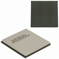
EP3SL150F1152C3N Altera, EP3SL150F1152C3N Datasheet - Page 269

EP3SL150F1152C3N
Manufacturer Part Number
EP3SL150F1152C3N
Description
IC STRATX III FPGA 150K 1152FBGA
Manufacturer
Altera
Series
Stratix® IIIr
Datasheets
1.EP3SL150F780C4N.pdf
(16 pages)
2.EP3SL150F780C4N.pdf
(332 pages)
3.EP3SL150F780C4N.pdf
(456 pages)
Specifications of EP3SL150F1152C3N
Number Of Logic Elements/cells
142500
Number Of Labs/clbs
5700
Total Ram Bits
6390
Number Of I /o
744
Voltage - Supply
0.86 V ~ 1.15 V
Mounting Type
Surface Mount
Operating Temperature
0°C ~ 85°C
Package / Case
1152-FBGA
For Use With
544-2568 - KIT DEVELOPMENT STRATIX III
Lead Free Status / RoHS Status
Lead free / RoHS Compliant
Number Of Gates
-
Other names
544-2408
EP3SL150F1152C3NES
EP3SL150F1152C3NES
Available stocks
Company
Part Number
Manufacturer
Quantity
Price
Company:
Part Number:
EP3SL150F1152C3N
Manufacturer:
ALTERA
Quantity:
490
- Current page: 269 of 456
- Download datasheet (7Mb)
Chapter 8: External Memory Interfaces in Stratix III Devices
Stratix III External Memory Interface Features
© March 2010 Altera Corporation
1
DLL
DQS phase-shift circuitry uses a DLL to dynamically measure the clock period
required by the DQS/CQ and CQn pin. The DLL, in turn, uses a frequency reference
to dynamically generate control signals for the delay chains in each of the DQS/CQ
and CQn pins, allowing it to compensate for PVT variations. The DQS delay settings
are Gray-coded to reduce jitter when the DLL updates the settings. The phase-shift
circuitry requires a maximum of 1280 clock cycles to lock and calculate the correct
input clock period when the DLL is in low jitter mode. Otherwise, only 256 clock
cycles are required. Do not send data during these clock cycles because there is no
guarantee it can be properly captured. As the settings from the DLL may not be stable
until this lock period has elapsed, you should be aware that anything using these
settings (including the leveling delay system) may be unstable during this period.
Use the DQS phase-shift circuitry for any memory interfaces that are less than
100 MHz. The DQS signal is shifted by 2.5 ns. Even if the DQS signal is not shifted
exactly to the middle of the DQ valid window, the I/O element should still be able to
capture the data in low frequency applications where a large amount of timing
margin is available.
There are four DLLs in a Stratix III device, located in each corner of the device. These
DLLs support a maximum of four unique frequencies, with each DLL running at one
frequency. Each DLL can have two outputs with different phase offsets, which allow
one Stratix III device to have eight different DLL phase shift settings.
shows the DLL and I/O bank locations in Stratix III devices from a package bottom
view.
Stratix III Device Handbook, Volume 1
Figure 8–11
8–21
Related parts for EP3SL150F1152C3N
Image
Part Number
Description
Manufacturer
Datasheet
Request
R

Part Number:
Description:
CYCLONE II STARTER KIT EP2C20N
Manufacturer:
Altera
Datasheet:

Part Number:
Description:
CPLD, EP610 Family, ECMOS Process, 300 Gates, 16 Macro Cells, 16 Reg., 16 User I/Os, 5V Supply, 35 Speed Grade, 24DIP
Manufacturer:
Altera Corporation
Datasheet:

Part Number:
Description:
CPLD, EP610 Family, ECMOS Process, 300 Gates, 16 Macro Cells, 16 Reg., 16 User I/Os, 5V Supply, 15 Speed Grade, 24DIP
Manufacturer:
Altera Corporation
Datasheet:

Part Number:
Description:
Manufacturer:
Altera Corporation
Datasheet:

Part Number:
Description:
CPLD, EP610 Family, ECMOS Process, 300 Gates, 16 Macro Cells, 16 Reg., 16 User I/Os, 5V Supply, 30 Speed Grade, 24DIP
Manufacturer:
Altera Corporation
Datasheet:

Part Number:
Description:
High-performance, low-power erasable programmable logic devices with 8 macrocells, 10ns
Manufacturer:
Altera Corporation
Datasheet:

Part Number:
Description:
High-performance, low-power erasable programmable logic devices with 8 macrocells, 7ns
Manufacturer:
Altera Corporation
Datasheet:

Part Number:
Description:
Classic EPLD
Manufacturer:
Altera Corporation
Datasheet:

Part Number:
Description:
High-performance, low-power erasable programmable logic devices with 8 macrocells, 10ns
Manufacturer:
Altera Corporation
Datasheet:

Part Number:
Description:
Manufacturer:
Altera Corporation
Datasheet:

Part Number:
Description:
Manufacturer:
Altera Corporation
Datasheet:

Part Number:
Description:
Manufacturer:
Altera Corporation
Datasheet:

Part Number:
Description:
CPLD, EP610 Family, ECMOS Process, 300 Gates, 16 Macro Cells, 16 Reg., 16 User I/Os, 5V Supply, 25 Speed Grade, 24DIP
Manufacturer:
Altera Corporation
Datasheet:


