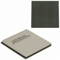
EP3SL150F1152C3N Altera, EP3SL150F1152C3N Datasheet - Page 265

EP3SL150F1152C3N
Manufacturer Part Number
EP3SL150F1152C3N
Description
IC STRATX III FPGA 150K 1152FBGA
Manufacturer
Altera
Series
Stratix® IIIr
Datasheets
1.EP3SL150F780C4N.pdf
(16 pages)
2.EP3SL150F780C4N.pdf
(332 pages)
3.EP3SL150F780C4N.pdf
(456 pages)
Specifications of EP3SL150F1152C3N
Number Of Logic Elements/cells
142500
Number Of Labs/clbs
5700
Total Ram Bits
6390
Number Of I /o
744
Voltage - Supply
0.86 V ~ 1.15 V
Mounting Type
Surface Mount
Operating Temperature
0°C ~ 85°C
Package / Case
1152-FBGA
For Use With
544-2568 - KIT DEVELOPMENT STRATIX III
Lead Free Status / RoHS Status
Lead free / RoHS Compliant
Number Of Gates
-
Other names
544-2408
EP3SL150F1152C3NES
EP3SL150F1152C3NES
Available stocks
Company
Part Number
Manufacturer
Quantity
Price
Company:
Part Number:
EP3SL150F1152C3N
Manufacturer:
ALTERA
Quantity:
490
- Current page: 265 of 456
- Download datasheet (7Mb)
Chapter 8: External Memory Interfaces in Stratix III Devices
Memory Interfaces Pin Support
Optional Parity, DM, BWSn, NWSn, ECC and QVLD Pins
Address and Control/Command Pins
© March 2010 Altera Corporation
In Stratix III devices, you can use any of the DQ pins from the same DQS/DQ group
for data as parity pins. The Stratix III device family supports parity in ×8/×9,
×16/×18, and ×32/×36 modes. There is one parity bit available per eight bits of data
pins. Use any of the DQ (or D) pins in the same DQS/DQ group as data for parity as
they are treated, configured, and generated like a DQ pin.
DM pins are only required when writing to DDR3, DDR2, DDR SDRAM, and
RLDRAM II devices. QDR II+ and QDR II SRAM devices use the BWSn (or NWSn in
the ×8 QDR II SRAM devices) signal to select which byte to write into the memory.
Each group of DQS and DQ signals in DDR3, DDR2, and DDR SDRAM devices
require a DM pin. There is one DM pin per RLDRAM II device and one BWSn pin per
9 bits of data in ×9, ×18, and ×36 QDR II+/QDR II SRAM. The ×8 QDR II SRAM
device has two BWSn pins per 8 data bits, which are referred to as NWSn pins.
A low signal on DM, NWSn, or BWSn indicates that the write is valid. If the
DM/BWSn/NWSn signal is high, the memory masks the DQ signals. If the system
does not require write data masking, connect the memory DM pins low to indicate
every write data is valid. You can use any of the DQ pins in the same DQS/DQ group
as write data for the DM/BWSn/NWSn signals. Generate the DM or BWSn signals
using DQ pins and configure the signals similar to the DQ (or D) output signals.
Stratix III devices do not support the DM signal in ×4 DDR3 SDRAM or in ×4 DDR2
SDRAM interfaces with differential DQS signaling.
Some DDR3, DDR2, and DDR SDRAM devices or modules support error correction
coding (ECC), which is a method of detecting and automatically correcting errors in
data transmission. In a 72-bit DDR3, DDR2, or DDR SDRAM interface, typically eight
ECC pins are used in addition to the 64 data pins. Connect the DDR3, DDR2, and
DDR SDRAM ECC pins to a Stratix III device DQS/DQ group. These signals are also
generated similar to DQ pins. The memory controller requires encoding and decoding
logic for ECC data. You can also use the extra byte of data for other error checking
methods.
QVLD pins are used in RLDRAM II and QDR II+ SRAM interfaces to indicate read
data availability. There is one QVLD pin per memory device. A high on QVLD
indicates that the memory is outputting the data requested. Similar to DQ inputs, this
signal is edge-aligned with the read clock signals (CQ/CQn in
QDR II+/QDR II SRAM and QK/QK# in RLDRAM II) and is sent half a clock cycle
before data starts coming out of the memory. The QVLD pin is not used in the
ALTMEMPHY megafunction solution for QDR II+ SRAM.
For more information about the parity, ECC, and QVLD pins as these pins are treated
as DQ pins refer to
Address and control/command signals are typically sent at a single data rate. The
only exception is in QDR II SRAM burst-of-two devices, where the read address must
be captured on the rising edge of the clock while the write address must be captured
on the falling edge of the clock by the memory. There is no special circuitry required
for the address and control/command pins. You can use any of the user I/O pins in
the same I/O bank as the data pins.
“Data and Data-Strobe/Clock Pins”
on
Stratix III Device Handbook, Volume 1
page
8–4.
8–17
Related parts for EP3SL150F1152C3N
Image
Part Number
Description
Manufacturer
Datasheet
Request
R

Part Number:
Description:
CYCLONE II STARTER KIT EP2C20N
Manufacturer:
Altera
Datasheet:

Part Number:
Description:
CPLD, EP610 Family, ECMOS Process, 300 Gates, 16 Macro Cells, 16 Reg., 16 User I/Os, 5V Supply, 35 Speed Grade, 24DIP
Manufacturer:
Altera Corporation
Datasheet:

Part Number:
Description:
CPLD, EP610 Family, ECMOS Process, 300 Gates, 16 Macro Cells, 16 Reg., 16 User I/Os, 5V Supply, 15 Speed Grade, 24DIP
Manufacturer:
Altera Corporation
Datasheet:

Part Number:
Description:
Manufacturer:
Altera Corporation
Datasheet:

Part Number:
Description:
CPLD, EP610 Family, ECMOS Process, 300 Gates, 16 Macro Cells, 16 Reg., 16 User I/Os, 5V Supply, 30 Speed Grade, 24DIP
Manufacturer:
Altera Corporation
Datasheet:

Part Number:
Description:
High-performance, low-power erasable programmable logic devices with 8 macrocells, 10ns
Manufacturer:
Altera Corporation
Datasheet:

Part Number:
Description:
High-performance, low-power erasable programmable logic devices with 8 macrocells, 7ns
Manufacturer:
Altera Corporation
Datasheet:

Part Number:
Description:
Classic EPLD
Manufacturer:
Altera Corporation
Datasheet:

Part Number:
Description:
High-performance, low-power erasable programmable logic devices with 8 macrocells, 10ns
Manufacturer:
Altera Corporation
Datasheet:

Part Number:
Description:
Manufacturer:
Altera Corporation
Datasheet:

Part Number:
Description:
Manufacturer:
Altera Corporation
Datasheet:

Part Number:
Description:
Manufacturer:
Altera Corporation
Datasheet:

Part Number:
Description:
CPLD, EP610 Family, ECMOS Process, 300 Gates, 16 Macro Cells, 16 Reg., 16 User I/Os, 5V Supply, 25 Speed Grade, 24DIP
Manufacturer:
Altera Corporation
Datasheet:


