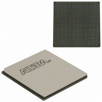
EP3SL150F1152C3N Altera, EP3SL150F1152C3N Datasheet - Page 263

EP3SL150F1152C3N
Manufacturer Part Number
EP3SL150F1152C3N
Description
IC STRATX III FPGA 150K 1152FBGA
Manufacturer
Altera
Series
Stratix® IIIr
Datasheets
1.EP3SL150F780C4N.pdf
(16 pages)
2.EP3SL150F780C4N.pdf
(332 pages)
3.EP3SL150F780C4N.pdf
(456 pages)
Specifications of EP3SL150F1152C3N
Number Of Logic Elements/cells
142500
Number Of Labs/clbs
5700
Total Ram Bits
6390
Number Of I /o
744
Voltage - Supply
0.86 V ~ 1.15 V
Mounting Type
Surface Mount
Operating Temperature
0°C ~ 85°C
Package / Case
1152-FBGA
For Use With
544-2568 - KIT DEVELOPMENT STRATIX III
Lead Free Status / RoHS Status
Lead free / RoHS Compliant
Number Of Gates
-
Other names
544-2408
EP3SL150F1152C3NES
EP3SL150F1152C3NES
Available stocks
Company
Part Number
Manufacturer
Quantity
Price
Company:
Part Number:
EP3SL150F1152C3N
Manufacturer:
ALTERA
Quantity:
490
- Current page: 263 of 456
- Download datasheet (7Mb)
Chapter 8: External Memory Interfaces in Stratix III Devices
Memory Interfaces Pin Support
Table 8–3. DQ/DQS Group in Stratix III Modular I/O Banks
Combining ×16/×18 DQS/DQ groups for ×36 QDR II+/QDR II SRAM Interface
© March 2010 Altera Corporation
24 pins
32 pins
40 pins
48 pins
Note to
(1) Some of the ×4 groups may use R
Modular I/O Bank
Table 8–1 on page
Table
Size
8–3:
f
1
8–5.
Similarly, in ×16/×18 mode, the I/O bank combines four adjacent ×4 DQS/DQ
groups to create a group with a maximum of 19 DQ pins (including parity or DM and
QVLD pins) and a pair of DQS/CQ and DQSn/CQn pins. In ×32/×36 mode, the I/O
bank combines eight adjacent ×4 DQS DQ groups together to create a group with a
maximum of 37 DQ pins (including parity or DM and QVLD pins) and a pair of
DQS/CQ and DQSn/CQn pins.
Stratix III modular I/O banks allow easy formation of the DQS/DQ groups. If all the
pins in the I/O banks are user I/O pins and are not used for programming, RUP/RDN
used for OCT calibration, or PLL clock output pins, you can divide the number of I/O
pins in the bank by six to get the maximum possible number of ×4 groups. You can
then divide that number by two, four, or eight to get the maximum possible number
of ×8/×9, ×16/×18, or ×32/×36, respectively (refer to
the pins in the I/O bank may be used for other functions.
This implementation combines two ×16/×18 DQS/DQ groups to interface with a ×36
QDR II+/QDR II SRAM device. The ×36 read data bus uses two ×16/×18 groups,
while the ×36 write data uses another two ×16/×18 groups or four ×8/×9 groups. The
CQ/CQn signal traces are split on the board trace to connect two pairs of DQS/CQn
pins in the FPGA. This is the only connection on the board that you need to change for
this implementation. Other QDR II+/QDR II SRAM interface rules for Stratix III
devices also apply for this implementation.
Altera’s ALTMEMPHY megafunction does not use the QVLD signal, so you can leave
the QVLD signal unconnected as in any QDR II+/QDR II SRAM interfaces in the
Stratix III devices.
For more information about the ALTMEMPHY megafunction, refer to the
ALTMEMPHY Megafunction User
Rules to Combine Groups
In 780- and 1152-pin package devices, there is at most one ×16/×18 group per I/O
sub-bank. You can combine ×16/×18 groups from a single side of the device for a ×36
interface. For devices that do not have four ×16/×18 groups in a single side of the
device to form two ×36 groups for read and write data, you can form one ×36 group
on one side of the device, and another ×36 group on the other side of the device. For
Maximum Possible
×4 Groups
Number of
UP
4
5
6
8
/R
DN
(1)
pins. You cannot use these groups if you use the Stratix III calibrated OCT feature, as described in
Maximum Possible
Number of ×8/×9
Groups
2
2
3
4
Guide.
Maximum Possible
Number of ×16/×18
Groups
1
1
1
2
Table
Stratix III Device Handbook, Volume 1
8–3). However, some of
Maximum Possible
Number of ×32/×36
Groups
0
0
0
1
8–15
Related parts for EP3SL150F1152C3N
Image
Part Number
Description
Manufacturer
Datasheet
Request
R

Part Number:
Description:
CYCLONE II STARTER KIT EP2C20N
Manufacturer:
Altera
Datasheet:

Part Number:
Description:
CPLD, EP610 Family, ECMOS Process, 300 Gates, 16 Macro Cells, 16 Reg., 16 User I/Os, 5V Supply, 35 Speed Grade, 24DIP
Manufacturer:
Altera Corporation
Datasheet:

Part Number:
Description:
CPLD, EP610 Family, ECMOS Process, 300 Gates, 16 Macro Cells, 16 Reg., 16 User I/Os, 5V Supply, 15 Speed Grade, 24DIP
Manufacturer:
Altera Corporation
Datasheet:

Part Number:
Description:
Manufacturer:
Altera Corporation
Datasheet:

Part Number:
Description:
CPLD, EP610 Family, ECMOS Process, 300 Gates, 16 Macro Cells, 16 Reg., 16 User I/Os, 5V Supply, 30 Speed Grade, 24DIP
Manufacturer:
Altera Corporation
Datasheet:

Part Number:
Description:
High-performance, low-power erasable programmable logic devices with 8 macrocells, 10ns
Manufacturer:
Altera Corporation
Datasheet:

Part Number:
Description:
High-performance, low-power erasable programmable logic devices with 8 macrocells, 7ns
Manufacturer:
Altera Corporation
Datasheet:

Part Number:
Description:
Classic EPLD
Manufacturer:
Altera Corporation
Datasheet:

Part Number:
Description:
High-performance, low-power erasable programmable logic devices with 8 macrocells, 10ns
Manufacturer:
Altera Corporation
Datasheet:

Part Number:
Description:
Manufacturer:
Altera Corporation
Datasheet:

Part Number:
Description:
Manufacturer:
Altera Corporation
Datasheet:

Part Number:
Description:
Manufacturer:
Altera Corporation
Datasheet:

Part Number:
Description:
CPLD, EP610 Family, ECMOS Process, 300 Gates, 16 Macro Cells, 16 Reg., 16 User I/Os, 5V Supply, 25 Speed Grade, 24DIP
Manufacturer:
Altera Corporation
Datasheet:


