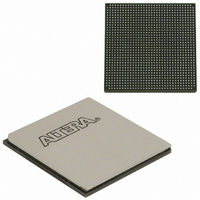
EP3SL150F1152C3N Altera, EP3SL150F1152C3N Datasheet - Page 240

EP3SL150F1152C3N
Manufacturer Part Number
EP3SL150F1152C3N
Description
IC STRATX III FPGA 150K 1152FBGA
Manufacturer
Altera
Series
Stratix® IIIr
Datasheets
1.EP3SL150F780C4N.pdf
(16 pages)
2.EP3SL150F780C4N.pdf
(332 pages)
3.EP3SL150F780C4N.pdf
(456 pages)
Specifications of EP3SL150F1152C3N
Number Of Logic Elements/cells
142500
Number Of Labs/clbs
5700
Total Ram Bits
6390
Number Of I /o
744
Voltage - Supply
0.86 V ~ 1.15 V
Mounting Type
Surface Mount
Operating Temperature
0°C ~ 85°C
Package / Case
1152-FBGA
For Use With
544-2568 - KIT DEVELOPMENT STRATIX III
Lead Free Status / RoHS Status
Lead free / RoHS Compliant
Number Of Gates
-
Other names
544-2408
EP3SL150F1152C3NES
EP3SL150F1152C3NES
Available stocks
Company
Part Number
Manufacturer
Quantity
Price
Company:
Part Number:
EP3SL150F1152C3N
Manufacturer:
ALTERA
Quantity:
490
- Current page: 240 of 456
- Download datasheet (7Mb)
7–36
Figure 7–24. LVDS I/O Standard Termination for Stratix III Devices
Notes to
(1) R
(2) Row I/O banks support true LVDS output buffers.
(3) Column and row I/O banks support LVDS_E_1R and LVDS_E_3R I/O standards using two single-ended output buffers.
Stratix III Device Handbook, Volume 1
P
=120 Ω for LVDS_E_1R, R
Figure
emulated LVDS Output
emulated LVDS Output
External On-Board
7–24:
OCT Receive
(Single-Ended
(Single-Ended
OCT Receive
LVDS_E_1R)
OCT Receive
LVDS_E_3R)
Termination
(True LVDS
Termination
with Three
with One
Network,
Network,
Resistor
Resistor
Output)
(2)
(3)
(3)
LVDS
The LVDS I/O standard is a differential high-speed, low-voltage swing, low-power,
general-purpose I/O interface standard. In Stratix III devices, the LVDS I/O standard
requires a 2.5-V V
standard in applications requiring high-bandwidth data transfer, backplane drivers,
and clock distribution. LVDS requires a 100-Ω termination resistor between the two
signals at the input buffer. Stratix III devices provide an optional 100-Ω differential
termination resistor in the device using on-chip differential termination.
Figure 7–24
row I/O banks.
P
=170 Ω , and R
Differential Outputs
Differential Outputs
Single-Ended Outputs
Single-Ended Outputs
shows the details of LVDS termination. The OCT R
S
=120 Ω for LVDS_E_3R.
CCIO
level. The LVDS input buffer requires 2.5-V V
External Resistor
Rp
External Resistor
Rs
Rs
Rp
(Note 1)
LVDS
50
50
50
50
50
50
50
50
100
Chapter 7: Stratix III Device I/O Features
100
100
100
Termination Schemes for I/O Standards
Differential Inputs
Differential Inputs
Differential Inputs
© July 2010 Altera Corporation
Stratix III OCT
Stratix III OCT
Differential Inputs
Stratix III OCT
D
is only available in
CCPD
. Use this
Related parts for EP3SL150F1152C3N
Image
Part Number
Description
Manufacturer
Datasheet
Request
R

Part Number:
Description:
CYCLONE II STARTER KIT EP2C20N
Manufacturer:
Altera
Datasheet:

Part Number:
Description:
CPLD, EP610 Family, ECMOS Process, 300 Gates, 16 Macro Cells, 16 Reg., 16 User I/Os, 5V Supply, 35 Speed Grade, 24DIP
Manufacturer:
Altera Corporation
Datasheet:

Part Number:
Description:
CPLD, EP610 Family, ECMOS Process, 300 Gates, 16 Macro Cells, 16 Reg., 16 User I/Os, 5V Supply, 15 Speed Grade, 24DIP
Manufacturer:
Altera Corporation
Datasheet:

Part Number:
Description:
Manufacturer:
Altera Corporation
Datasheet:

Part Number:
Description:
CPLD, EP610 Family, ECMOS Process, 300 Gates, 16 Macro Cells, 16 Reg., 16 User I/Os, 5V Supply, 30 Speed Grade, 24DIP
Manufacturer:
Altera Corporation
Datasheet:

Part Number:
Description:
High-performance, low-power erasable programmable logic devices with 8 macrocells, 10ns
Manufacturer:
Altera Corporation
Datasheet:

Part Number:
Description:
High-performance, low-power erasable programmable logic devices with 8 macrocells, 7ns
Manufacturer:
Altera Corporation
Datasheet:

Part Number:
Description:
Classic EPLD
Manufacturer:
Altera Corporation
Datasheet:

Part Number:
Description:
High-performance, low-power erasable programmable logic devices with 8 macrocells, 10ns
Manufacturer:
Altera Corporation
Datasheet:

Part Number:
Description:
Manufacturer:
Altera Corporation
Datasheet:

Part Number:
Description:
Manufacturer:
Altera Corporation
Datasheet:

Part Number:
Description:
Manufacturer:
Altera Corporation
Datasheet:

Part Number:
Description:
CPLD, EP610 Family, ECMOS Process, 300 Gates, 16 Macro Cells, 16 Reg., 16 User I/Os, 5V Supply, 25 Speed Grade, 24DIP
Manufacturer:
Altera Corporation
Datasheet:


