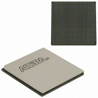
EP3SL150F1152C3N Altera, EP3SL150F1152C3N Datasheet - Page 230

EP3SL150F1152C3N
Manufacturer Part Number
EP3SL150F1152C3N
Description
IC STRATX III FPGA 150K 1152FBGA
Manufacturer
Altera
Series
Stratix® IIIr
Datasheets
1.EP3SL150F780C4N.pdf
(16 pages)
2.EP3SL150F780C4N.pdf
(332 pages)
3.EP3SL150F780C4N.pdf
(456 pages)
Specifications of EP3SL150F1152C3N
Number Of Logic Elements/cells
142500
Number Of Labs/clbs
5700
Total Ram Bits
6390
Number Of I /o
744
Voltage - Supply
0.86 V ~ 1.15 V
Mounting Type
Surface Mount
Operating Temperature
0°C ~ 85°C
Package / Case
1152-FBGA
For Use With
544-2568 - KIT DEVELOPMENT STRATIX III
Lead Free Status / RoHS Status
Lead free / RoHS Compliant
Number Of Gates
-
Other names
544-2408
EP3SL150F1152C3NES
EP3SL150F1152C3NES
Available stocks
Company
Part Number
Manufacturer
Quantity
Price
Company:
Part Number:
EP3SL150F1152C3N
Manufacturer:
ALTERA
Quantity:
490
- Current page: 230 of 456
- Download datasheet (7Mb)
7–26
LVDS Input On-Chip Termination (R
Table 7–11. On-Chip Differential Termination in Quartus II Software Assignment Editor
Stratix III Device Handbook, Volume 1
Input Termination (Accepts wildcards/groups)
Output Termination
f
1
Assignment Name
Stratix III devices support OCT for differential LVDS input buffers with a nominal
resistance value of 10 Ω, as shown in
banks when V
OCT R
PLL_L[1,4]_CLK[p,n], and PLL_R[1,4]_CLK[p,n] on the row I/O banks of the
Stratix III devices do not support OCT R
CLK[0,2,9,11][p,n] on row I/O banks support OCT R
CLK[4,5,6,7][p,n] and CLK[12,13,14,15][p,n] on column I/O banks do not
support OCT R
Figure 7–12. Differential Input On-Chip Termination
For more information about OCT R
with DPA in Stratix III Devices
Table 7–11
software Assignment Editor.
You must set the V
the LVDS input buffer is powered by V
D.
The dedicated clock input pairs CLK[1,3,8,10][p,n],
lists the assignment name and its value for OCT R
Transmitter
CCIO
D
.
and V
CCIO
D
)
to 2.5 V when OCT R
CCPD
are set to 2.5 V. The column I/O banks do not support
chapter.
Parallel 50 Ω with calibration
Differential
Series 25 Ω without
calibration
Series 50 Ω without
calibration
Series 25 Ω with calibration
Series 40 Ω with calibration
Series 50 Ω with calibration
Series 60 Ω with calibration
D
Allowed Values
, refer to the
Figure
Z
Z
CCPD
O
O
D
= 50
= 50
. Dedicated clock input pairs
.
D
7–12. You can enable OCT R
is used for the LVDS input buffer, even if
High Speed Differential I/O Interfaces
Chapter 7: Stratix III Device I/O Features
D
. Dedicated clock input pairs
Input buffers for single-ended
and differential-HSTL/SSTL
standards
Input buffers for LVDS
receivers on row I/O banks.
Output buffers for
single-ended LVTTL/LVCMOS
and HSTL/SSTL standards as
well as differential HSTL/SSTL
standards.
100
D
© July 2010 Altera Corporation
in the Quartus II
Receiver
Applies To
D
in row I/O
OCT Support
Related parts for EP3SL150F1152C3N
Image
Part Number
Description
Manufacturer
Datasheet
Request
R

Part Number:
Description:
CYCLONE II STARTER KIT EP2C20N
Manufacturer:
Altera
Datasheet:

Part Number:
Description:
CPLD, EP610 Family, ECMOS Process, 300 Gates, 16 Macro Cells, 16 Reg., 16 User I/Os, 5V Supply, 35 Speed Grade, 24DIP
Manufacturer:
Altera Corporation
Datasheet:

Part Number:
Description:
CPLD, EP610 Family, ECMOS Process, 300 Gates, 16 Macro Cells, 16 Reg., 16 User I/Os, 5V Supply, 15 Speed Grade, 24DIP
Manufacturer:
Altera Corporation
Datasheet:

Part Number:
Description:
Manufacturer:
Altera Corporation
Datasheet:

Part Number:
Description:
CPLD, EP610 Family, ECMOS Process, 300 Gates, 16 Macro Cells, 16 Reg., 16 User I/Os, 5V Supply, 30 Speed Grade, 24DIP
Manufacturer:
Altera Corporation
Datasheet:

Part Number:
Description:
High-performance, low-power erasable programmable logic devices with 8 macrocells, 10ns
Manufacturer:
Altera Corporation
Datasheet:

Part Number:
Description:
High-performance, low-power erasable programmable logic devices with 8 macrocells, 7ns
Manufacturer:
Altera Corporation
Datasheet:

Part Number:
Description:
Classic EPLD
Manufacturer:
Altera Corporation
Datasheet:

Part Number:
Description:
High-performance, low-power erasable programmable logic devices with 8 macrocells, 10ns
Manufacturer:
Altera Corporation
Datasheet:

Part Number:
Description:
Manufacturer:
Altera Corporation
Datasheet:

Part Number:
Description:
Manufacturer:
Altera Corporation
Datasheet:

Part Number:
Description:
Manufacturer:
Altera Corporation
Datasheet:

Part Number:
Description:
CPLD, EP610 Family, ECMOS Process, 300 Gates, 16 Macro Cells, 16 Reg., 16 User I/Os, 5V Supply, 25 Speed Grade, 24DIP
Manufacturer:
Altera Corporation
Datasheet:


