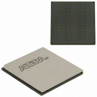
EP3SL150F1152C3N Altera, EP3SL150F1152C3N Datasheet - Page 209

EP3SL150F1152C3N
Manufacturer Part Number
EP3SL150F1152C3N
Description
IC STRATX III FPGA 150K 1152FBGA
Manufacturer
Altera
Series
Stratix® IIIr
Datasheets
1.EP3SL150F780C4N.pdf
(16 pages)
2.EP3SL150F780C4N.pdf
(332 pages)
3.EP3SL150F780C4N.pdf
(456 pages)
Specifications of EP3SL150F1152C3N
Number Of Logic Elements/cells
142500
Number Of Labs/clbs
5700
Total Ram Bits
6390
Number Of I /o
744
Voltage - Supply
0.86 V ~ 1.15 V
Mounting Type
Surface Mount
Operating Temperature
0°C ~ 85°C
Package / Case
1152-FBGA
For Use With
544-2568 - KIT DEVELOPMENT STRATIX III
Lead Free Status / RoHS Status
Lead free / RoHS Compliant
Number Of Gates
-
Other names
544-2408
EP3SL150F1152C3NES
EP3SL150F1152C3NES
Available stocks
Company
Part Number
Manufacturer
Quantity
Price
Company:
Part Number:
EP3SL150F1152C3N
Manufacturer:
ALTERA
Quantity:
490
- Current page: 209 of 456
- Download datasheet (7Mb)
Chapter 7: Stratix III Device I/O Features
Stratix III I/O Banks
Table 7–2. I/O Standards and Voltage Levels for Stratix III Devices
Stratix III I/O Banks
© July 2010
LVPECL
Notes to
(1) V
(2) Single-ended HSTL/SSTL, differential SSTL/HSTL, and LVDS input buffers are powered by V
(3) V
(4) Column and row I/O banks support LVPECL I/O standards for input operation only on dedicated clock input pins. Clock inputs on column I/O
(5) Row I/O banks support LVDS outputs using a dedicated output buffer. Column and row I/O banks support emulated LVDS outputs using two
(6) Row I/O banks support RSDS and mini-LVDS I/O standards using a true LVDS output buffer without a resistor network.
(7) Column and row I/O banks support emulated-RSDS and mini-LVDS I/O standards using two single-ended output buffers with one-resistor
(8) The emulated differential output standard that supports the tri-state feature includes: LVDS_E_1R, LVDS_E_3R, RSDS_E_1R, RSDS_E_3R,
I/O Standard
use V
are powered by V
single-ended output buffers and external one-resistor (LVDS_E_1R) and a three-resistor (LVDS_E_3R) network.
(RSDS_E_1R and mini-LVDS_E_1R) and three-resistor (RSDS_E_3R and mini-LVDS_E_3R) networks.
Mini_LVDS_E_1R, and Mini_LVDS_E_3R.
CC PD
CC CLKIN
Table
is either 2.5 V, 3.0 V, or 3.3 V. For V
CC IO
powers the Column I/O bank dedicated clock input pins when configured as differential inputs. Clock input pins on the Column I/O banks
Altera Corporation
when configured as single-ended inputs.
f
f
7–2:
1
C CC LKIN
For detailed electrical characteristics of each I/O standard, refer to the
Switching Characteristics of Stratix III Devices
Stratix III devices contain up to 24 I/O banks, as shown in
banks contain true differential input and output buffers and dedicated circuitry to
support differential standards at speeds up to 1.6 Gbps.
Every I/O bank in Stratix III devices can support high-performance external memory
interfaces with dedicated circuitry. The I/O pins are organized in pairs to support
differential standards. Each I/O pin pair can support both differential input and
output buffers. The only exceptions are the
CLK[1, 3, 8, 10][p,n], PLL_L[1,4]_CLK[p,n], and PLL_R[1,4]_CLK[p,n] pins,
which support differential or single-ended input operations, these pins do not
support output operations.
Pins that do not support output operations do not support the programmable current
strength, programmable slew rate, programmable pull-up, bus hold, open-drain, or
on-chip series termination (OCT R
For the number of channels available for the LVDS I/O standard, refer to the
High-Speed Differential I/O Interface with DPA in Stratix III Devices
Standard
Support
when configured as differential clock input. Differential clock inputs in row I/O are powered by V
—
Column I/O
CC IO
Banks
= 3.3 V, V
(4)
Input Operation
CC PD
=3.3 V. For V
Row I/O
Banks
(4)
V
CCIO
(V)
S
CC IO
) options.
Output Operation
Column
Banks
= 3.0 V, V
(Note
I/O
—
1),
chapter.
CC PD
Row I/O
(3)
Banks
= 3.0 V. For V
—
(Part 3 of 3)
C CP D
.
Voltage)
V
Driver
C CP D
(Pre-
2.5
CC IO
(V)
Stratix III Device Handbook, Volume 1
Figure
= 2.5 V or less, V
Voltage)
V
chapter.
(Input
REF
Ref
7–1. The row I/O
—
(V)
CC PD
DC and
C CP D
.
V
Termination
TT
= 2.5 V.
Voltage)
(V) (Board
—
7–5
Related parts for EP3SL150F1152C3N
Image
Part Number
Description
Manufacturer
Datasheet
Request
R

Part Number:
Description:
CYCLONE II STARTER KIT EP2C20N
Manufacturer:
Altera
Datasheet:

Part Number:
Description:
CPLD, EP610 Family, ECMOS Process, 300 Gates, 16 Macro Cells, 16 Reg., 16 User I/Os, 5V Supply, 35 Speed Grade, 24DIP
Manufacturer:
Altera Corporation
Datasheet:

Part Number:
Description:
CPLD, EP610 Family, ECMOS Process, 300 Gates, 16 Macro Cells, 16 Reg., 16 User I/Os, 5V Supply, 15 Speed Grade, 24DIP
Manufacturer:
Altera Corporation
Datasheet:

Part Number:
Description:
Manufacturer:
Altera Corporation
Datasheet:

Part Number:
Description:
CPLD, EP610 Family, ECMOS Process, 300 Gates, 16 Macro Cells, 16 Reg., 16 User I/Os, 5V Supply, 30 Speed Grade, 24DIP
Manufacturer:
Altera Corporation
Datasheet:

Part Number:
Description:
High-performance, low-power erasable programmable logic devices with 8 macrocells, 10ns
Manufacturer:
Altera Corporation
Datasheet:

Part Number:
Description:
High-performance, low-power erasable programmable logic devices with 8 macrocells, 7ns
Manufacturer:
Altera Corporation
Datasheet:

Part Number:
Description:
Classic EPLD
Manufacturer:
Altera Corporation
Datasheet:

Part Number:
Description:
High-performance, low-power erasable programmable logic devices with 8 macrocells, 10ns
Manufacturer:
Altera Corporation
Datasheet:

Part Number:
Description:
Manufacturer:
Altera Corporation
Datasheet:

Part Number:
Description:
Manufacturer:
Altera Corporation
Datasheet:

Part Number:
Description:
Manufacturer:
Altera Corporation
Datasheet:

Part Number:
Description:
CPLD, EP610 Family, ECMOS Process, 300 Gates, 16 Macro Cells, 16 Reg., 16 User I/Os, 5V Supply, 25 Speed Grade, 24DIP
Manufacturer:
Altera Corporation
Datasheet:


