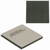
EP3SL150F1152C3N Altera, EP3SL150F1152C3N Datasheet - Page 200

EP3SL150F1152C3N
Manufacturer Part Number
EP3SL150F1152C3N
Description
IC STRATX III FPGA 150K 1152FBGA
Manufacturer
Altera
Series
Stratix® IIIr
Datasheets
1.EP3SL150F780C4N.pdf
(16 pages)
2.EP3SL150F780C4N.pdf
(332 pages)
3.EP3SL150F780C4N.pdf
(456 pages)
Specifications of EP3SL150F1152C3N
Number Of Logic Elements/cells
142500
Number Of Labs/clbs
5700
Total Ram Bits
6390
Number Of I /o
744
Voltage - Supply
0.86 V ~ 1.15 V
Mounting Type
Surface Mount
Operating Temperature
0°C ~ 85°C
Package / Case
1152-FBGA
For Use With
544-2568 - KIT DEVELOPMENT STRATIX III
Lead Free Status / RoHS Status
Lead free / RoHS Compliant
Number Of Gates
-
Other names
544-2408
EP3SL150F1152C3NES
EP3SL150F1152C3NES
Available stocks
Company
Part Number
Manufacturer
Quantity
Price
Company:
Part Number:
EP3SL150F1152C3N
Manufacturer:
ALTERA
Quantity:
490
- Current page: 200 of 456
- Download datasheet (7Mb)
6–52
PLL Cascading and Clock Network Guidelines
Spread-Spectrum Tracking
PLL Specifications
Stratix III Device Handbook, Volume 1
f
When cascading PLLs in Stratix III devices, the source (upstream) PLL must have a
low-bandwidth setting while the destination (downstream) PLL must have a
high-bandwidth setting. There must be no overlap of the bandwidth ranges of the two
PLLs.
To ensure that the memory interface’s PLL is configured correctly in the external
memory interface design, the following settings are required:
■
■
Stratix III devices can accept a spread-spectrum input with typical modulation
frequencies. However, the device cannot automatically detect that the input is a
spread-spectrum signal. Instead, the input signal looks like deterministic jitter at the
input of PLL. Stratix III PLLs can track a spread-spectrum input clock as long as it is
within the input-jitter tolerance specifications and the modulation frequency of the
input clock is below the PLL bandwidth which is specified in the fitter report.
Stratix III devices cannot internally generate spread-spectrum clocks.
For information about PLL timing specifications, refer to the
Characteristics of Stratix III Devices
The PLL used to generate the memory output clock signals and write data/clock
signals must be set to No compensation mode to minimize output clock jitter.
The reference input clock signal to the PLL must be driven by the dedicated clock
input pin located adjacent to the PLL, or from the clock output signal from the
adjacent PLL. To minimize output clock jitter, the reference input clock pin must
not be routed through the core using global or regional clock networks. If reference
clock is cascaded from another PLL, that upstream PLL must be configured in No
compensation mode and Low bandwidth mode.
chapter.
Chapter 6: Clock Networks and PLLs in Stratix III Devices
DC and Switching
© July 2010 Altera Corporation
PLLs in Stratix III Devices
Related parts for EP3SL150F1152C3N
Image
Part Number
Description
Manufacturer
Datasheet
Request
R

Part Number:
Description:
CYCLONE II STARTER KIT EP2C20N
Manufacturer:
Altera
Datasheet:

Part Number:
Description:
CPLD, EP610 Family, ECMOS Process, 300 Gates, 16 Macro Cells, 16 Reg., 16 User I/Os, 5V Supply, 35 Speed Grade, 24DIP
Manufacturer:
Altera Corporation
Datasheet:

Part Number:
Description:
CPLD, EP610 Family, ECMOS Process, 300 Gates, 16 Macro Cells, 16 Reg., 16 User I/Os, 5V Supply, 15 Speed Grade, 24DIP
Manufacturer:
Altera Corporation
Datasheet:

Part Number:
Description:
Manufacturer:
Altera Corporation
Datasheet:

Part Number:
Description:
CPLD, EP610 Family, ECMOS Process, 300 Gates, 16 Macro Cells, 16 Reg., 16 User I/Os, 5V Supply, 30 Speed Grade, 24DIP
Manufacturer:
Altera Corporation
Datasheet:

Part Number:
Description:
High-performance, low-power erasable programmable logic devices with 8 macrocells, 10ns
Manufacturer:
Altera Corporation
Datasheet:

Part Number:
Description:
High-performance, low-power erasable programmable logic devices with 8 macrocells, 7ns
Manufacturer:
Altera Corporation
Datasheet:

Part Number:
Description:
Classic EPLD
Manufacturer:
Altera Corporation
Datasheet:

Part Number:
Description:
High-performance, low-power erasable programmable logic devices with 8 macrocells, 10ns
Manufacturer:
Altera Corporation
Datasheet:

Part Number:
Description:
Manufacturer:
Altera Corporation
Datasheet:

Part Number:
Description:
Manufacturer:
Altera Corporation
Datasheet:

Part Number:
Description:
Manufacturer:
Altera Corporation
Datasheet:

Part Number:
Description:
CPLD, EP610 Family, ECMOS Process, 300 Gates, 16 Macro Cells, 16 Reg., 16 User I/Os, 5V Supply, 25 Speed Grade, 24DIP
Manufacturer:
Altera Corporation
Datasheet:


