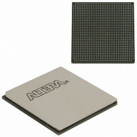
EP3SL150F1152C3N Altera, EP3SL150F1152C3N Datasheet - Page 197

EP3SL150F1152C3N
Manufacturer Part Number
EP3SL150F1152C3N
Description
IC STRATX III FPGA 150K 1152FBGA
Manufacturer
Altera
Series
Stratix® IIIr
Datasheets
1.EP3SL150F780C4N.pdf
(16 pages)
2.EP3SL150F780C4N.pdf
(332 pages)
3.EP3SL150F780C4N.pdf
(456 pages)
Specifications of EP3SL150F1152C3N
Number Of Logic Elements/cells
142500
Number Of Labs/clbs
5700
Total Ram Bits
6390
Number Of I /o
744
Voltage - Supply
0.86 V ~ 1.15 V
Mounting Type
Surface Mount
Operating Temperature
0°C ~ 85°C
Package / Case
1152-FBGA
For Use With
544-2568 - KIT DEVELOPMENT STRATIX III
Lead Free Status / RoHS Status
Lead free / RoHS Compliant
Number Of Gates
-
Other names
544-2408
EP3SL150F1152C3NES
EP3SL150F1152C3NES
Available stocks
Company
Part Number
Manufacturer
Quantity
Price
Company:
Part Number:
EP3SL150F1152C3N
Manufacturer:
ALTERA
Quantity:
490
- Current page: 197 of 456
- Download datasheet (7Mb)
Chapter 6: Clock Networks and PLLs in Stratix III Devices
PLLs in Stratix III Devices
Table 6–20. PLL Counter Settings
Table 6–21. Dynamic Phase-Shifting Control Signals (Part 1 of 2)
© July 2010
Notes to
(1) Most significant bit (MSB).
(2) Least significant bit (LSB).
(3) Counter-bypass bit.
PHASECOUNTERSELECT
[3:0]
PHASEUPDOWN
PHASESTEP
LSB
(2)
X
0
Signal Name
Table
[1]
X
X
Altera Corporation
6–20:
1
[2]
X
X
Bypassing PLL
Bypassing a PLL counter results in a multiply (m counter) or a divide (n and C0 to C9
counters) factor of one.
Table 6–20
To bypass any of the PLL counters, set the bypass bit to 1. The values on the other bits
are ignored. To bypass the VCO post-scale counter (K), set the corresponding bit to 1.
Dynamic Phase-Shifting
The dynamic phase-shifting feature allows the output phases of individual PLL
outputs to be dynamically adjusted relative to each other and to the reference clock
without the need to send serial data through the scan chain of the corresponding PLL.
This feature simplifies the interface and allows you to quickly adjust clock-to-out (t
delays by changing the output clock phase-shift in real time. This adjustment is
achieved by incrementing or decrementing the VCO phase-tap selection to a given C
counter or to the M counter. The phase is shifted by 1/8 of the VCO frequency at a
time. The output clocks are active during this phase-reconfiguration process.
Table 6–21
[3]
X
X
Counter select. Four bits decoded
to select either the M or one of the
C counters for phase adjustment.
One address maps to select all
C counters. This signal is
registered in the PLL on the rising
edge of SCANCLK.
Selects dynamic phase shift
direction; 1= UP; 0= DOWN. Signal
is registered in the PLL on the
rising edge of SCANCLK.
Logic high enables dynamic phase
shifting.
[4]
lists the settings for bypassing the counters in Stratix III PLLs.
X
X
lists the control signals that are used for dynamic phase-shifting.
Description
PLL Scan Chain Bits [0..10] Settings
[5]
X
X
[6]
X
X
[7]
X
X
[8]
Logic array or I/O pins
Logic array or I/O pin
Logic array or I/O pin
X
X
[9]
X
X
Source
MSB
1
0
(1)
(3)
(3)
Stratix III Device Handbook, Volume 1
PLL counter bypassed
PLL counter not bypassed
because bit 10 (MSB) is set to 0
PLL reconfiguration circuit
PLL reconfiguration circuit
PLL reconfiguration circuit
Description
Destination
6–49
CO
)
Related parts for EP3SL150F1152C3N
Image
Part Number
Description
Manufacturer
Datasheet
Request
R

Part Number:
Description:
CYCLONE II STARTER KIT EP2C20N
Manufacturer:
Altera
Datasheet:

Part Number:
Description:
CPLD, EP610 Family, ECMOS Process, 300 Gates, 16 Macro Cells, 16 Reg., 16 User I/Os, 5V Supply, 35 Speed Grade, 24DIP
Manufacturer:
Altera Corporation
Datasheet:

Part Number:
Description:
CPLD, EP610 Family, ECMOS Process, 300 Gates, 16 Macro Cells, 16 Reg., 16 User I/Os, 5V Supply, 15 Speed Grade, 24DIP
Manufacturer:
Altera Corporation
Datasheet:

Part Number:
Description:
Manufacturer:
Altera Corporation
Datasheet:

Part Number:
Description:
CPLD, EP610 Family, ECMOS Process, 300 Gates, 16 Macro Cells, 16 Reg., 16 User I/Os, 5V Supply, 30 Speed Grade, 24DIP
Manufacturer:
Altera Corporation
Datasheet:

Part Number:
Description:
High-performance, low-power erasable programmable logic devices with 8 macrocells, 10ns
Manufacturer:
Altera Corporation
Datasheet:

Part Number:
Description:
High-performance, low-power erasable programmable logic devices with 8 macrocells, 7ns
Manufacturer:
Altera Corporation
Datasheet:

Part Number:
Description:
Classic EPLD
Manufacturer:
Altera Corporation
Datasheet:

Part Number:
Description:
High-performance, low-power erasable programmable logic devices with 8 macrocells, 10ns
Manufacturer:
Altera Corporation
Datasheet:

Part Number:
Description:
Manufacturer:
Altera Corporation
Datasheet:

Part Number:
Description:
Manufacturer:
Altera Corporation
Datasheet:

Part Number:
Description:
Manufacturer:
Altera Corporation
Datasheet:

Part Number:
Description:
CPLD, EP610 Family, ECMOS Process, 300 Gates, 16 Macro Cells, 16 Reg., 16 User I/Os, 5V Supply, 25 Speed Grade, 24DIP
Manufacturer:
Altera Corporation
Datasheet:


