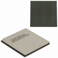
EP3SL150F1152C3N Altera, EP3SL150F1152C3N Datasheet - Page 189

EP3SL150F1152C3N
Manufacturer Part Number
EP3SL150F1152C3N
Description
IC STRATX III FPGA 150K 1152FBGA
Manufacturer
Altera
Series
Stratix® IIIr
Datasheets
1.EP3SL150F780C4N.pdf
(16 pages)
2.EP3SL150F780C4N.pdf
(332 pages)
3.EP3SL150F780C4N.pdf
(456 pages)
Specifications of EP3SL150F1152C3N
Number Of Logic Elements/cells
142500
Number Of Labs/clbs
5700
Total Ram Bits
6390
Number Of I /o
744
Voltage - Supply
0.86 V ~ 1.15 V
Mounting Type
Surface Mount
Operating Temperature
0°C ~ 85°C
Package / Case
1152-FBGA
For Use With
544-2568 - KIT DEVELOPMENT STRATIX III
Lead Free Status / RoHS Status
Lead free / RoHS Compliant
Number Of Gates
-
Other names
544-2408
EP3SL150F1152C3NES
EP3SL150F1152C3NES
Available stocks
Company
Part Number
Manufacturer
Quantity
Price
Company:
Part Number:
EP3SL150F1152C3N
Manufacturer:
ALTERA
Quantity:
490
- Current page: 189 of 456
- Download datasheet (7Mb)
Chapter 6: Clock Networks and PLLs in Stratix III Devices
PLLs in Stratix III Devices
Phase-Shift Implementation
© July 2010
Altera Corporation
Phase shift is used to implement a robust solution for clock delays in Stratix III
devices. Phase shift is implemented by using a combination of the VCO phase output
and the counter starting time. The VCO phase output and counter starting time is the
most accurate method of inserting delays, since it is based purely on counter settings,
which are independent of process, voltage, and temperature.
You can phase-shift the output clocks from the Stratix III PLLs in either of these two
resolutions:
■
■
Fine-resolution phase shifts are implemented by allowing any of the output counters
(C[n..0]) or the m counter to use any of the eight phases of the VCO as the reference
clock. This allows you to adjust the delay time with a fine resolution. The minimum
delay time that you can insert using this method is defined by
Equation 6–1.
where f
For example, if f
156.25 ps. This phase shift is defined by the PLL operating frequency, which is
governed by the reference clock frequency and the counter settings.
Coarse-resolution phase shifts are implemented by delaying the start of the counters
for a predetermined number of counter clocks. You can express coarse phase shift as
shown in
Equation 6–2.
where C is the count value set for the counter delay time (this is the initial setting in
the PLL usage section of the compilation report in the Quartus II software). If the
initial value is 1, C – 1 = 0° phase shift.
Figure 6–39
the VCO phase taps method. The eight phases from the VCO are shown and labeled
for reference. For this example, CLK0 is based off the 0phase from the VCO and has
the C value for the counter set to one. The CLK0 signal is divided by four, two VCO
clocks for high time and two VCO clocks for low time. CLK1 is based off the 135°
phase tap from the VCO and also has the C value for the counter set to one. The CLK1
signal is also divided by 4. In this case, the two clocks are offset by 3Φ
off the 0phase from the VCO but has the C value for the counter set to three. This
arrangement creates a delay of 2Φ
Fine resolution using VCO phase taps
Coarse resolution using counter starting time
REF
Equation
is the input reference clock frequency.
shows an example of phase-shift insertion with the fine resolution using
REF
is 100 MHz, n is 1, and m is 8, then f
6–2.
fine
coarse
coarse
=
1
8
=
T
(two complete VCO periods).
VCO
C 1
f
=
V
co
8f
1
VCO
=
(C 1)N
=
Mf
8Mf
REF
N
REF
VCO
is 800 MHz and Φ
Stratix III Device Handbook, Volume 1
Equation
fine
. CLK2 is based
6–1.
fine
equals
6–41
Related parts for EP3SL150F1152C3N
Image
Part Number
Description
Manufacturer
Datasheet
Request
R

Part Number:
Description:
CYCLONE II STARTER KIT EP2C20N
Manufacturer:
Altera
Datasheet:

Part Number:
Description:
CPLD, EP610 Family, ECMOS Process, 300 Gates, 16 Macro Cells, 16 Reg., 16 User I/Os, 5V Supply, 35 Speed Grade, 24DIP
Manufacturer:
Altera Corporation
Datasheet:

Part Number:
Description:
CPLD, EP610 Family, ECMOS Process, 300 Gates, 16 Macro Cells, 16 Reg., 16 User I/Os, 5V Supply, 15 Speed Grade, 24DIP
Manufacturer:
Altera Corporation
Datasheet:

Part Number:
Description:
Manufacturer:
Altera Corporation
Datasheet:

Part Number:
Description:
CPLD, EP610 Family, ECMOS Process, 300 Gates, 16 Macro Cells, 16 Reg., 16 User I/Os, 5V Supply, 30 Speed Grade, 24DIP
Manufacturer:
Altera Corporation
Datasheet:

Part Number:
Description:
High-performance, low-power erasable programmable logic devices with 8 macrocells, 10ns
Manufacturer:
Altera Corporation
Datasheet:

Part Number:
Description:
High-performance, low-power erasable programmable logic devices with 8 macrocells, 7ns
Manufacturer:
Altera Corporation
Datasheet:

Part Number:
Description:
Classic EPLD
Manufacturer:
Altera Corporation
Datasheet:

Part Number:
Description:
High-performance, low-power erasable programmable logic devices with 8 macrocells, 10ns
Manufacturer:
Altera Corporation
Datasheet:

Part Number:
Description:
Manufacturer:
Altera Corporation
Datasheet:

Part Number:
Description:
Manufacturer:
Altera Corporation
Datasheet:

Part Number:
Description:
Manufacturer:
Altera Corporation
Datasheet:

Part Number:
Description:
CPLD, EP610 Family, ECMOS Process, 300 Gates, 16 Macro Cells, 16 Reg., 16 User I/Os, 5V Supply, 25 Speed Grade, 24DIP
Manufacturer:
Altera Corporation
Datasheet:


