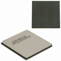
EP3SL150F1152C3N Altera, EP3SL150F1152C3N Datasheet - Page 169

EP3SL150F1152C3N
Manufacturer Part Number
EP3SL150F1152C3N
Description
IC STRATX III FPGA 150K 1152FBGA
Manufacturer
Altera
Series
Stratix® IIIr
Datasheets
1.EP3SL150F780C4N.pdf
(16 pages)
2.EP3SL150F780C4N.pdf
(332 pages)
3.EP3SL150F780C4N.pdf
(456 pages)
Specifications of EP3SL150F1152C3N
Number Of Logic Elements/cells
142500
Number Of Labs/clbs
5700
Total Ram Bits
6390
Number Of I /o
744
Voltage - Supply
0.86 V ~ 1.15 V
Mounting Type
Surface Mount
Operating Temperature
0°C ~ 85°C
Package / Case
1152-FBGA
For Use With
544-2568 - KIT DEVELOPMENT STRATIX III
Lead Free Status / RoHS Status
Lead free / RoHS Compliant
Number Of Gates
-
Other names
544-2408
EP3SL150F1152C3NES
EP3SL150F1152C3NES
Available stocks
Company
Part Number
Manufacturer
Quantity
Price
Company:
Part Number:
EP3SL150F1152C3N
Manufacturer:
ALTERA
Quantity:
490
- Current page: 169 of 456
- Download datasheet (7Mb)
Chapter 6: Clock Networks and PLLs in Stratix III Devices
PLLs in Stratix III Devices
Figure 6–19. Stratix III PLL Block Diagram
Notes to
(1) The number of post-scale counters is 7 for Left/Right PLLs and 10 for Top/Bottom PLLs.
(2) This is the VCO post-scale counter
(3) The FBOUT port is fed by the
(4) The global (GCLK) or regional (RCLK) clock input can be driven by an output from another PLL, a clock pin-driven global or regional clock, or
© July 2010
VCO frequency reported by the Quartus II software is divided by the post-scale counter
through a clock control block provided the clock control block is fed by an output from another PLL or a pin driven dedicated global or regional
clock. An internally generated global signal or general purpose I/O pin cannot drive the PLL.
Dedicated Clock inputs
from adjacent PLL
Figure
GCLK/RCLK
Cascade input
Altera Corporation
pfdena
from pins
6–19:
(4)
The loop filter converts these up and down signals to a voltage that is used to bias the
VCO. The loop filter also removes glitches from the charge pump and prevents
voltage overshoot, which filters the jitter on the VCO. The voltage from the loop filter
determines how fast the VCO operates. A divide counter (m) is inserted in the
feedback loop to increase the VCO frequency above the input reference frequency.
VCO frequency (f
reference clock (f
counter (N). Therefore, the feedback clock (f
locked to the f
The VCO output from Left/Right PLLs can feed seven post-scale counters (C[0..6]),
while the corresponding VCO output from Top/Bottom PLLs can feed ten post-scale
counters (C[0..9]). These post-scale counters allow a number of harmonically
related frequencies to be produced by the PLL.
Figure 6–19
Stratix III PLL.
PLL Clock I/O Pins
Each Top/Bottom PLL supports six clock I/O pins, organized as three pairs of pins:
■
■
■
4
1st pair: 2 single-ended I/O or 1 differential I/O
2nd pair: 2 single-ended I/O, 1 differential external feedback input (FBp/FBn), or
1 single-ended external feedback input (FBp)
3rd pair: 2 single-ended I/O or 1 differential input
M
counter in Stratix III PLLs.
inclk0
inclk1
K
.
Switchover
If the design enables this ÷2 counter, the device can use a VCO frequency range of 300 to 650 MHz. The
Clock
Block
shows a simplified block diagram of the major components of the
REF
REF
that is applied to the other input of the PFD.
VCO
÷n
) to the PFD is equal to the input clock (f
clkswitch
clkbad0
clkbad1
activeclock
) is equal to (m) times the input reference clock (f
PFD
Circuit
Lock
CP
locked
LF
VCO
FB
) applied to one input of the PFD is
8
K
no compensation mode
ZDB, External feedback modes
LVDS Compensation mode
Source Synchronous, normal modes
.
÷2
(2)
To DPA block on
Left/Right PLLs
8
/2, /4
8
Stratix III Device Handbook, Volume 1
IN
) divided by the pre-scale
÷C0
÷C1
÷C2
÷C3
÷Cn
÷m
(1)
REF
). The input
Casade output
to adjacent PLL
FBIN
DIFFIOCLK network
GCLK/RCLK network
GCLKs
RCLKs
DIFFIOCLK from
Left/Right PLLs
LOAD_EN from
Left/Right PLLs
FBOUT (3)
External
memory
interface DLL
External clock
outputs
6–21
Related parts for EP3SL150F1152C3N
Image
Part Number
Description
Manufacturer
Datasheet
Request
R

Part Number:
Description:
CYCLONE II STARTER KIT EP2C20N
Manufacturer:
Altera
Datasheet:

Part Number:
Description:
CPLD, EP610 Family, ECMOS Process, 300 Gates, 16 Macro Cells, 16 Reg., 16 User I/Os, 5V Supply, 35 Speed Grade, 24DIP
Manufacturer:
Altera Corporation
Datasheet:

Part Number:
Description:
CPLD, EP610 Family, ECMOS Process, 300 Gates, 16 Macro Cells, 16 Reg., 16 User I/Os, 5V Supply, 15 Speed Grade, 24DIP
Manufacturer:
Altera Corporation
Datasheet:

Part Number:
Description:
Manufacturer:
Altera Corporation
Datasheet:

Part Number:
Description:
CPLD, EP610 Family, ECMOS Process, 300 Gates, 16 Macro Cells, 16 Reg., 16 User I/Os, 5V Supply, 30 Speed Grade, 24DIP
Manufacturer:
Altera Corporation
Datasheet:

Part Number:
Description:
High-performance, low-power erasable programmable logic devices with 8 macrocells, 10ns
Manufacturer:
Altera Corporation
Datasheet:

Part Number:
Description:
High-performance, low-power erasable programmable logic devices with 8 macrocells, 7ns
Manufacturer:
Altera Corporation
Datasheet:

Part Number:
Description:
Classic EPLD
Manufacturer:
Altera Corporation
Datasheet:

Part Number:
Description:
High-performance, low-power erasable programmable logic devices with 8 macrocells, 10ns
Manufacturer:
Altera Corporation
Datasheet:

Part Number:
Description:
Manufacturer:
Altera Corporation
Datasheet:

Part Number:
Description:
Manufacturer:
Altera Corporation
Datasheet:

Part Number:
Description:
Manufacturer:
Altera Corporation
Datasheet:

Part Number:
Description:
CPLD, EP610 Family, ECMOS Process, 300 Gates, 16 Macro Cells, 16 Reg., 16 User I/Os, 5V Supply, 25 Speed Grade, 24DIP
Manufacturer:
Altera Corporation
Datasheet:


