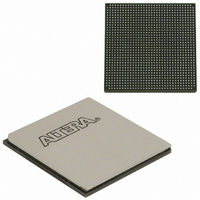
EP3SL150F1152C3N Altera, EP3SL150F1152C3N Datasheet - Page 162

EP3SL150F1152C3N
Manufacturer Part Number
EP3SL150F1152C3N
Description
IC STRATX III FPGA 150K 1152FBGA
Manufacturer
Altera
Series
Stratix® IIIr
Datasheets
1.EP3SL150F780C4N.pdf
(16 pages)
2.EP3SL150F780C4N.pdf
(332 pages)
3.EP3SL150F780C4N.pdf
(456 pages)
Specifications of EP3SL150F1152C3N
Number Of Logic Elements/cells
142500
Number Of Labs/clbs
5700
Total Ram Bits
6390
Number Of I /o
744
Voltage - Supply
0.86 V ~ 1.15 V
Mounting Type
Surface Mount
Operating Temperature
0°C ~ 85°C
Package / Case
1152-FBGA
For Use With
544-2568 - KIT DEVELOPMENT STRATIX III
Lead Free Status / RoHS Status
Lead free / RoHS Compliant
Number Of Gates
-
Other names
544-2408
EP3SL150F1152C3NES
EP3SL150F1152C3NES
Available stocks
Company
Part Number
Manufacturer
Quantity
Price
Company:
Part Number:
EP3SL150F1152C3N
Manufacturer:
ALTERA
Quantity:
490
- Current page: 162 of 456
- Download datasheet (7Mb)
6–14
Clock Control Block
Stratix III Device Handbook, Volume 1
Figure 6–11. Clock Input Multiplexer Logic for L2, L3, T1, T2, B1, B2, R2, and R3 PLLs
Notes to
(1) The input clock multiplexing is controlled through a configuration file (.sof or .pof) only and cannot be dynamically
(2) n=0 for L2 and L3 PLLs; n=4 for B1 and B2 PLLs; n=8 for R2 and R3 PLLs, and n=12 for T1 and T2 PLLs.
(3) The global (GCLK) or regional (RCLK) clock input can be driven by an output from another PLL, a pin-driven global
Figure 6–12. Clock Input Multiplexer Logic for L1, L4, R1, and R4 PLLs
Notes to
(1) Dedicated clock input pins to PLLs - L1, L4, R1 and R4, respectively. For example, PLL_L1_CLK is the dedicated
(2) The global (GCLK) or regional (RCLK) clock input can be driven by an output from another PLL, a pin-driven global
(3) The center clock pins can feed the corner PLLs on the same side directly, through a dedicated path. However, these
Every global and regional clock network has its own clock control block. The control
block provides the following features:
■
■
■
You can select the clock source for the global clock select block either statically or
dynamically. You can either statically select the clock source using a setting in the
Quartus II software, or you can dynamically select the clock source using internal
logic to drive the multiplexer select inputs. When selecting the clock source
dynamically, you can either select two PLL outputs (such as CLK0 or CLK1), or a
combination of clock pins or PLL outputs.
Clock source selection (dynamic selection for global clocks)
Global clock multiplexing
Clock power down (static or dynamic clock enable or disable)
controlled in user mode operation.
or regional clock, or through a clock control block provided the clock control block is fed by an output from another
PLL or a pin driven dedicated global or regional clock. An internally generated global signal or general purpose I/O
pin cannot drive the PLL.
clock input for PLL_L1.
or regional clock, or through a clock control block provided the clock control block is fed by an output from another
PLL or a pin driven dedicated global or regional clock. An internally generated global signal or general purpose I/O
pin cannot drive the PLL.
paths may not be fully compensated.
Figure
Figure
GCLK / RCLK input (3)
6–11:
6–12:
Adjacent PLL output
clk[n+3..n] (2)
PLL_<L1/L4/R1/R4>_CLK (1)
CLK[0..3] or CLK[8..11] (3)
GCLK/RCLK (2)
4
4
4
4
Chapter 6: Clock Networks and PLLs in Stratix III Devices
(1)
(1)
inclk0
inclk1
Clock Networks in Stratix III Devices
To the clock
switchover block
© July 2010 Altera Corporation
inclk0
inclk1
Related parts for EP3SL150F1152C3N
Image
Part Number
Description
Manufacturer
Datasheet
Request
R

Part Number:
Description:
CYCLONE II STARTER KIT EP2C20N
Manufacturer:
Altera
Datasheet:

Part Number:
Description:
CPLD, EP610 Family, ECMOS Process, 300 Gates, 16 Macro Cells, 16 Reg., 16 User I/Os, 5V Supply, 35 Speed Grade, 24DIP
Manufacturer:
Altera Corporation
Datasheet:

Part Number:
Description:
CPLD, EP610 Family, ECMOS Process, 300 Gates, 16 Macro Cells, 16 Reg., 16 User I/Os, 5V Supply, 15 Speed Grade, 24DIP
Manufacturer:
Altera Corporation
Datasheet:

Part Number:
Description:
Manufacturer:
Altera Corporation
Datasheet:

Part Number:
Description:
CPLD, EP610 Family, ECMOS Process, 300 Gates, 16 Macro Cells, 16 Reg., 16 User I/Os, 5V Supply, 30 Speed Grade, 24DIP
Manufacturer:
Altera Corporation
Datasheet:

Part Number:
Description:
High-performance, low-power erasable programmable logic devices with 8 macrocells, 10ns
Manufacturer:
Altera Corporation
Datasheet:

Part Number:
Description:
High-performance, low-power erasable programmable logic devices with 8 macrocells, 7ns
Manufacturer:
Altera Corporation
Datasheet:

Part Number:
Description:
Classic EPLD
Manufacturer:
Altera Corporation
Datasheet:

Part Number:
Description:
High-performance, low-power erasable programmable logic devices with 8 macrocells, 10ns
Manufacturer:
Altera Corporation
Datasheet:

Part Number:
Description:
Manufacturer:
Altera Corporation
Datasheet:

Part Number:
Description:
Manufacturer:
Altera Corporation
Datasheet:

Part Number:
Description:
Manufacturer:
Altera Corporation
Datasheet:

Part Number:
Description:
CPLD, EP610 Family, ECMOS Process, 300 Gates, 16 Macro Cells, 16 Reg., 16 User I/Os, 5V Supply, 25 Speed Grade, 24DIP
Manufacturer:
Altera Corporation
Datasheet:


