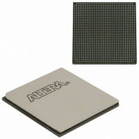
EP3SL150F1152C3N Altera, EP3SL150F1152C3N Datasheet - Page 103

EP3SL150F1152C3N
Manufacturer Part Number
EP3SL150F1152C3N
Description
IC STRATX III FPGA 150K 1152FBGA
Manufacturer
Altera
Series
Stratix® IIIr
Datasheets
1.EP3SL150F780C4N.pdf
(16 pages)
2.EP3SL150F780C4N.pdf
(332 pages)
3.EP3SL150F780C4N.pdf
(456 pages)
Specifications of EP3SL150F1152C3N
Number Of Logic Elements/cells
142500
Number Of Labs/clbs
5700
Total Ram Bits
6390
Number Of I /o
744
Voltage - Supply
0.86 V ~ 1.15 V
Mounting Type
Surface Mount
Operating Temperature
0°C ~ 85°C
Package / Case
1152-FBGA
For Use With
544-2568 - KIT DEVELOPMENT STRATIX III
Lead Free Status / RoHS Status
Lead free / RoHS Compliant
Number Of Gates
-
Other names
544-2408
EP3SL150F1152C3NES
EP3SL150F1152C3NES
Available stocks
Company
Part Number
Manufacturer
Quantity
Price
Company:
Part Number:
EP3SL150F1152C3N
Manufacturer:
ALTERA
Quantity:
490
- Current page: 103 of 456
- Download datasheet (7Mb)
Chapter 4: TriMatrix Embedded Memory Blocks in Stratix III Devices
Design Considerations
Figure 4–21. Mixed Port Read During Write: Old Data Mode
Note to
(1)
Power-Up Conditions and Memory Initialization
© May 2009 Altera Corporation
A0
Figure
(old data) is the old data at address
4–21:
f
1
q_b_(asyn)
address_b
address_a
clk_a&b
bytenna
data_a
rdenb
wrena
For more details about how to implement the desired behavior, read-during-write
behavior is controlled via the RAM MegaWizard Plug-In Manager refer to the
Megafunction User
You should select don’t care mode if you do not use old data mode. This increases the
flexibility in the type of memory block used, if you do not assign block type when
instantiating a memory block. You may also get potential performance gain by
selecting don’t care mode.
Figure 4–21
behavior for the old data mode. In don’t care mode, the old data shown in the figure is
simply replaced with “don’t cares”.
Mixed-port read-during-write using two different clocks in simple-dual port RAM
with old data output is supported via emulation. The Quartus II software takes two
memory blocks to implement the widest width mode.
M9K and M144K memory block outputs power up to zero (cleared), regardless of
whether the output registers are used or bypassed. MLABs power up to zero if output
registers are used and power up reading the memory contents if output registers are
not used. However, the actual RAM cells power up to an unknown state. Therefore,
after power-up, if an address is read before being written, the output from the read
operation is undefined because the contents are not initialized.
All memory blocks support initialization via .mif file. You can create .mif files in the
Quartus II software and specify their use with the RAM MegaWizard Plug-In
Manager when instantiating a memory in your design. Even if a memory is
pre-initialized (for example, by a .mif file), it still powers up with its outputs cleared.
For more information about .mif files, refer to the
the
Quartus II
A0
shows a sample functional waveform of mixed-port read-during-write
Handbook.
and
AAAA
11
A0 (old data)
A1
Guide.
(old data) is the old data at address
BBBB
01
A0
A0
AAAA
(Note 1)
CCCC
10
AABB
DDDD
A1(old data)
A1
.
RAM Megafunction User Guide
EEEE
11
A1
A1
DDDD
Stratix III Device Handbook, Volume 1
FFFF
EEEE
RAM
and
4–23
Related parts for EP3SL150F1152C3N
Image
Part Number
Description
Manufacturer
Datasheet
Request
R

Part Number:
Description:
CYCLONE II STARTER KIT EP2C20N
Manufacturer:
Altera
Datasheet:

Part Number:
Description:
CPLD, EP610 Family, ECMOS Process, 300 Gates, 16 Macro Cells, 16 Reg., 16 User I/Os, 5V Supply, 35 Speed Grade, 24DIP
Manufacturer:
Altera Corporation
Datasheet:

Part Number:
Description:
CPLD, EP610 Family, ECMOS Process, 300 Gates, 16 Macro Cells, 16 Reg., 16 User I/Os, 5V Supply, 15 Speed Grade, 24DIP
Manufacturer:
Altera Corporation
Datasheet:

Part Number:
Description:
Manufacturer:
Altera Corporation
Datasheet:

Part Number:
Description:
CPLD, EP610 Family, ECMOS Process, 300 Gates, 16 Macro Cells, 16 Reg., 16 User I/Os, 5V Supply, 30 Speed Grade, 24DIP
Manufacturer:
Altera Corporation
Datasheet:

Part Number:
Description:
High-performance, low-power erasable programmable logic devices with 8 macrocells, 10ns
Manufacturer:
Altera Corporation
Datasheet:

Part Number:
Description:
High-performance, low-power erasable programmable logic devices with 8 macrocells, 7ns
Manufacturer:
Altera Corporation
Datasheet:

Part Number:
Description:
Classic EPLD
Manufacturer:
Altera Corporation
Datasheet:

Part Number:
Description:
High-performance, low-power erasable programmable logic devices with 8 macrocells, 10ns
Manufacturer:
Altera Corporation
Datasheet:

Part Number:
Description:
Manufacturer:
Altera Corporation
Datasheet:

Part Number:
Description:
Manufacturer:
Altera Corporation
Datasheet:

Part Number:
Description:
Manufacturer:
Altera Corporation
Datasheet:

Part Number:
Description:
CPLD, EP610 Family, ECMOS Process, 300 Gates, 16 Macro Cells, 16 Reg., 16 User I/Os, 5V Supply, 25 Speed Grade, 24DIP
Manufacturer:
Altera Corporation
Datasheet:


