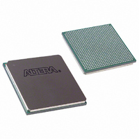
EP3SL150F780C4N Altera, EP3SL150F780C4N Datasheet - Page 97

EP3SL150F780C4N
Manufacturer Part Number
EP3SL150F780C4N
Description
IC STRATIX III FPGA 150K 780FBGA
Manufacturer
Altera
Series
Stratix® IIIr
Datasheets
1.EP3SL150F780C4N.pdf
(16 pages)
2.EP3SL150F780C4N.pdf
(332 pages)
3.EP3SL150F780C4N.pdf
(456 pages)
4.EP3SL150F780C4N.pdf
(341 pages)
Specifications of EP3SL150F780C4N
Number Of Logic Elements/cells
142500
Number Of Labs/clbs
5700
Total Ram Bits
6390
Number Of I /o
488
Voltage - Supply
0.86 V ~ 1.15 V
Mounting Type
Surface Mount
Operating Temperature
0°C ~ 85°C
Package / Case
780-FBGA
Family Name
Stratix III
Number Of Logic Blocks/elements
142500
# I/os (max)
488
Frequency (max)
450MHz
Process Technology
65nm
Operating Supply Voltage (typ)
1.1V
Logic Cells
142500
Ram Bits
6543360
Operating Supply Voltage (min)
1.05V
Operating Supply Voltage (max)
1.15V
Operating Temp Range
0C to 85C
Operating Temperature Classification
Commercial
Mounting
Surface Mount
Pin Count
780
Package Type
FC-FBGA
For Use With
544-2568 - KIT DEVELOPMENT STRATIX III
Lead Free Status / RoHS Status
Lead free / RoHS Compliant
Number Of Gates
-
Lead Free Status / Rohs Status
Compliant
Other names
544-2403
EP3SL150F780C4NES
EP3SL150F780C4NES
Available stocks
Company
Part Number
Manufacturer
Quantity
Price
Company:
Part Number:
EP3SL150F780C4N
Manufacturer:
ALTERA
Quantity:
3 000
- EP3SL150F780C4N PDF datasheet
- EP3SL150F780C4N PDF datasheet #2
- EP3SL150F780C4N PDF datasheet #3
- EP3SL150F780C4N PDF datasheet #4
- Current page: 97 of 456
- Download datasheet (7Mb)
Chapter 4: TriMatrix Embedded Memory Blocks in Stratix III Devices
Overview
Figure 4–16. Stratix III True Dual-Port Timing Waveform
Shift-Register Mode
© May 2009 Altera Corporation
q_a (asynch)
q_b (asynch)
address_a
address_b
wren_a
wren_b
data_a
clk_a
clk_b
din-1
an-1
doutn-1
All Stratix III memory blocks support shift register mode. Embedded memory block
configurations can implement shift registers for digital signal processing (DSP)
applications, such as finite impulse response (FIR) filters, pseudo-random number
generators, multi-channel filtering, and auto- and cross-correlation functions. These
and other DSP applications require local data storage, traditionally implemented with
standard flipflops that quickly exhaust many logic cells for large shift registers. A
more efficient alternative is to use embedded memory as a shift-register block, which
saves logic cell and routing resources.
The size of a shift register (w × m × n) is determined by the input data width (w), the
length of the taps (m), and the number of taps (n). You can cascade memory blocks to
implement larger shift registers.
bn
din-1
din
an
doutn
din
b0
a0
dout0
a1
dout0
dout1
b1
a2
dout2
a3
dout3
dout1
b2
din4
a4
Stratix III Device Handbook, Volume 1
din4
din5
a5
dout2
din5
b3
din6
a6
4–17
Related parts for EP3SL150F780C4N
Image
Part Number
Description
Manufacturer
Datasheet
Request
R

Part Number:
Description:
CYCLONE II STARTER KIT EP2C20N
Manufacturer:
Altera
Datasheet:

Part Number:
Description:
CPLD, EP610 Family, ECMOS Process, 300 Gates, 16 Macro Cells, 16 Reg., 16 User I/Os, 5V Supply, 35 Speed Grade, 24DIP
Manufacturer:
Altera Corporation
Datasheet:

Part Number:
Description:
CPLD, EP610 Family, ECMOS Process, 300 Gates, 16 Macro Cells, 16 Reg., 16 User I/Os, 5V Supply, 15 Speed Grade, 24DIP
Manufacturer:
Altera Corporation
Datasheet:

Part Number:
Description:
Manufacturer:
Altera Corporation
Datasheet:

Part Number:
Description:
CPLD, EP610 Family, ECMOS Process, 300 Gates, 16 Macro Cells, 16 Reg., 16 User I/Os, 5V Supply, 30 Speed Grade, 24DIP
Manufacturer:
Altera Corporation
Datasheet:

Part Number:
Description:
High-performance, low-power erasable programmable logic devices with 8 macrocells, 10ns
Manufacturer:
Altera Corporation
Datasheet:

Part Number:
Description:
High-performance, low-power erasable programmable logic devices with 8 macrocells, 7ns
Manufacturer:
Altera Corporation
Datasheet:

Part Number:
Description:
Classic EPLD
Manufacturer:
Altera Corporation
Datasheet:

Part Number:
Description:
High-performance, low-power erasable programmable logic devices with 8 macrocells, 10ns
Manufacturer:
Altera Corporation
Datasheet:

Part Number:
Description:
Manufacturer:
Altera Corporation
Datasheet:

Part Number:
Description:
Manufacturer:
Altera Corporation
Datasheet:

Part Number:
Description:
Manufacturer:
Altera Corporation
Datasheet:

Part Number:
Description:
CPLD, EP610 Family, ECMOS Process, 300 Gates, 16 Macro Cells, 16 Reg., 16 User I/Os, 5V Supply, 25 Speed Grade, 24DIP
Manufacturer:
Altera Corporation
Datasheet:


