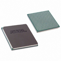
EP3SL150F780C4N Altera, EP3SL150F780C4N Datasheet - Page 417

EP3SL150F780C4N
Manufacturer Part Number
EP3SL150F780C4N
Description
IC STRATIX III FPGA 150K 780FBGA
Manufacturer
Altera
Series
Stratix® IIIr
Datasheets
1.EP3SL150F780C4N.pdf
(16 pages)
2.EP3SL150F780C4N.pdf
(332 pages)
3.EP3SL150F780C4N.pdf
(456 pages)
4.EP3SL150F780C4N.pdf
(341 pages)
Specifications of EP3SL150F780C4N
Number Of Logic Elements/cells
142500
Number Of Labs/clbs
5700
Total Ram Bits
6390
Number Of I /o
488
Voltage - Supply
0.86 V ~ 1.15 V
Mounting Type
Surface Mount
Operating Temperature
0°C ~ 85°C
Package / Case
780-FBGA
Family Name
Stratix III
Number Of Logic Blocks/elements
142500
# I/os (max)
488
Frequency (max)
450MHz
Process Technology
65nm
Operating Supply Voltage (typ)
1.1V
Logic Cells
142500
Ram Bits
6543360
Operating Supply Voltage (min)
1.05V
Operating Supply Voltage (max)
1.15V
Operating Temp Range
0C to 85C
Operating Temperature Classification
Commercial
Mounting
Surface Mount
Pin Count
780
Package Type
FC-FBGA
For Use With
544-2568 - KIT DEVELOPMENT STRATIX III
Lead Free Status / RoHS Status
Lead free / RoHS Compliant
Number Of Gates
-
Lead Free Status / Rohs Status
Compliant
Other names
544-2403
EP3SL150F780C4NES
EP3SL150F780C4NES
Available stocks
Company
Part Number
Manufacturer
Quantity
Price
Company:
Part Number:
EP3SL150F780C4N
Manufacturer:
ALTERA
Quantity:
3 000
- EP3SL150F780C4N PDF datasheet
- EP3SL150F780C4N PDF datasheet #2
- EP3SL150F780C4N PDF datasheet #3
- EP3SL150F780C4N PDF datasheet #4
- Current page: 417 of 456
- Download datasheet (7Mb)
Chapter 13: IEEE 1149.1 (JTAG) Boundary-Scan Testing in Stratix III Devices
IEEE Std. 1149.1 BST Circuitry (Disabling)
IEEE Std. 1149.1 BST Circuitry (Disabling)
IEEE Std. 1149.1 BST Guidelines
© July 2010
Altera Corporation
1
The IEEE Std. 1149.1 BST circuitry for Stratix III devices is enabled upon device
power-up. Because the IEEE Std. 1149.1 BST circuitry is used for BST or in-circuit
reconfiguration, you must enable the circuitry only at specific times as mentioned in,
“IEEE Std. 1149.1 BST Circuitry” on page
If you are not using the IEEE Std. 1149.1 circuitry in Stratix III, you should
permanently disable the circuitry to ensure that you do not inadvertently enable it
when it is not required.
Table 13–7
circuitry in Stratix III devices.
Table 13–7. Disabling IEEE Std. 1149.1 Circuitry
Use the following guidelines when performing boundary-scan testing with IEEE Std.
1149.1 devices:
■
Note to
(1) There is no software option to disable JTAG in Stratix III devices. The JTAG pins are dedicated.
If the “10...” pattern does not shift out of the instruction register through the TDO
pin during the first clock cycle of the SHIFT_IR state, the TAP controller did not
reach the proper state. To solve this problem, try one of the following procedures:
■
■
Do NOT use the following private instructions as they may render the device
inoperable:
11 0001 0000
00 1100 1001
11 0001 0011
11 0001 0111
You should take precautions to avoid invoking these instructions at any time.
Verify that the TAP controller has reached the SHIFT_IR state correctly. To
advance the TAP controller to the SHIFT_IR state, return to the RESET state
and send the code 01100 to the TMS pin.
Check the connections to the V
pins on the device.
Table
lists the pin connections necessary for disabling the IEEE Std. 1149.1
13–7:
JTAG Pins
TRST
TMS
TCK
TDI
TDO
(1)
CC
, GND, JTAG, and dedicated configuration
13–18.
Connection for Disabling
V
V
CC PD
CC PD
Stratix III Device Handbook, Volume 1
supply of Bank 1A
supply of Bank 1A
Leave open
GND
GND
13–19
Related parts for EP3SL150F780C4N
Image
Part Number
Description
Manufacturer
Datasheet
Request
R

Part Number:
Description:
CYCLONE II STARTER KIT EP2C20N
Manufacturer:
Altera
Datasheet:

Part Number:
Description:
CPLD, EP610 Family, ECMOS Process, 300 Gates, 16 Macro Cells, 16 Reg., 16 User I/Os, 5V Supply, 35 Speed Grade, 24DIP
Manufacturer:
Altera Corporation
Datasheet:

Part Number:
Description:
CPLD, EP610 Family, ECMOS Process, 300 Gates, 16 Macro Cells, 16 Reg., 16 User I/Os, 5V Supply, 15 Speed Grade, 24DIP
Manufacturer:
Altera Corporation
Datasheet:

Part Number:
Description:
Manufacturer:
Altera Corporation
Datasheet:

Part Number:
Description:
CPLD, EP610 Family, ECMOS Process, 300 Gates, 16 Macro Cells, 16 Reg., 16 User I/Os, 5V Supply, 30 Speed Grade, 24DIP
Manufacturer:
Altera Corporation
Datasheet:

Part Number:
Description:
High-performance, low-power erasable programmable logic devices with 8 macrocells, 10ns
Manufacturer:
Altera Corporation
Datasheet:

Part Number:
Description:
High-performance, low-power erasable programmable logic devices with 8 macrocells, 7ns
Manufacturer:
Altera Corporation
Datasheet:

Part Number:
Description:
Classic EPLD
Manufacturer:
Altera Corporation
Datasheet:

Part Number:
Description:
High-performance, low-power erasable programmable logic devices with 8 macrocells, 10ns
Manufacturer:
Altera Corporation
Datasheet:

Part Number:
Description:
Manufacturer:
Altera Corporation
Datasheet:

Part Number:
Description:
Manufacturer:
Altera Corporation
Datasheet:

Part Number:
Description:
Manufacturer:
Altera Corporation
Datasheet:

Part Number:
Description:
CPLD, EP610 Family, ECMOS Process, 300 Gates, 16 Macro Cells, 16 Reg., 16 User I/Os, 5V Supply, 25 Speed Grade, 24DIP
Manufacturer:
Altera Corporation
Datasheet:


