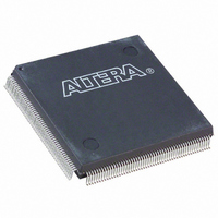
EP1K30QC208-3N Altera, EP1K30QC208-3N Datasheet - Page 41

EP1K30QC208-3N
Manufacturer Part Number
EP1K30QC208-3N
Description
IC ACEX 1K FPGA 30K 208-PQFP
Manufacturer
Altera
Series
ACEX-1K®r
Datasheet
1.EP1K10TC100-3N.pdf
(86 pages)
Specifications of EP1K30QC208-3N
Number Of Logic Elements/cells
1728
Number Of Labs/clbs
216
Total Ram Bits
24576
Number Of I /o
147
Number Of Gates
119000
Voltage - Supply
2.375 V ~ 2.625 V
Mounting Type
Surface Mount
Operating Temperature
0°C ~ 85°C
Package / Case
208-MQFP, 208-PQFP
Family Name
ACEX™ 1K
Number Of Usable Gates
30000
Number Of Logic Blocks/elements
1728
# I/os (max)
147
Frequency (max)
200MHz
Process Technology
CMOS
Operating Supply Voltage (typ)
2.5V
Logic Cells
1728
Ram Bits
24576
Device System Gates
119000
Operating Supply Voltage (min)
2.375V
Operating Supply Voltage (max)
2.625V
Operating Temp Range
0C to 70C
Operating Temperature Classification
Commercial
Mounting
Surface Mount
Pin Count
208
Package Type
PQFP
Lead Free Status / RoHS Status
Lead free / RoHS Compliant
Other names
544-1836
EP1K30QC208-3N
EP1K30QC208-3N
Available stocks
Company
Part Number
Manufacturer
Quantity
Price
Company:
Part Number:
EP1K30QC208-3N
Manufacturer:
ALTERA42
Quantity:
4 571
Part Number:
EP1K30QC208-3N
Manufacturer:
ALTERA/阿尔特拉
Quantity:
20 000
Altera Corporation
Power
Sequencing &
Hot-Socketing
The VCCINT pins must always be connected to a 2.5-V power supply.
With a 2.5-V V
V, and 5.0-V inputs. The VCCIO pins can be connected to either a 2.5-V or
3.3-V power supply, depending on the output requirements. When the
VCCIO pins are connected to a 2.5-V power supply, the output levels are
compatible with 2.5-V systems. When the VCCIO pins are connected to a
3.3-V power supply, the output high is at 3.3 V and is therefore compatible
with 3.3-V or 5.0-V systems. Devices operating with V
than 3.0 V achieve a faster timing delay of t
Table 13
Notes:
(1)
(2)
Open-drain output pins on ACEX 1K devices (with a pull-up resistor to
the 5.0-V supply) can drive 5.0-V CMOS input pins that require a higher
V
When the pin is inactive, the resistor will pull up the trace to 5.0 V, thereby
meeting the CMOS V
low or tri-state; it will never drive high. The rise time is dependent on the
value of the pull-up resistor and load impedance. The I
specification should be considered when selecting a pull-up resistor.
Because ACEX 1K devices can be used in a mixed-voltage environment,
they have been designed specifically to tolerate any possible power-up
sequence. The V
order.
Signals can be driven into ACEX 1K devices before and during power up
without damaging the device. Additionally, ACEX 1K devices do not
drive out during power up. Once operating conditions are reached,
ACEX 1K devices operate as specified by the user.
Table 13. ACEX 1K MultiVolt I/O Support
IH
than LVTTL. When the open-drain pin is active, it will drive low.
The PCI clamping diode must be disabled on an input which is driven with a
voltage higher than V
When V
tolerant inputs.
V
CCIO
2.5
3.3
summarizes ACEX 1K MultiVolt I/O support.
(V)
CCIO
CCINT
= 3.3 V, an ACEX 1K device can drive a 2.5-V device that has 3.3-V
CCIO
ACEX 1K Programmable Logic Device Family Data Sheet
level, input voltages are compatible with 2.5-V, 3.3-
2.5
OH
v
v
and V
CCIO
Input Signal (V)
requirement. The open-drain pin will only drive
.
CCINT
v
3.3
v
(1)
power planes can be powered in any
v
v
5.0
(1)
(1)
OD2
v
instead of t
2.5
v
(2)
Output Signal (V)
CCIO
OL
3.3
v
current
OD1
levels higher
.
5.0
v
41
13


