EP1C6T144C8 Altera, EP1C6T144C8 Datasheet - Page 44
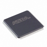
EP1C6T144C8
Manufacturer Part Number
EP1C6T144C8
Description
IC CYCLONE FPGA 5980 LE 144-TQFP
Manufacturer
Altera
Series
Cyclone®r
Datasheet
1.EP1C3T144C8.pdf
(106 pages)
Specifications of EP1C6T144C8
Number Of Logic Elements/cells
5980
Number Of Labs/clbs
598
Total Ram Bits
92160
Number Of I /o
98
Voltage - Supply
1.425 V ~ 1.575 V
Mounting Type
Surface Mount
Operating Temperature
0°C ~ 85°C
Package / Case
144-TQFP, 144-VQFP
Family Name
Cyclone®
Number Of Logic Blocks/elements
5980
# I/os (max)
98
Frequency (max)
275.03MHz
Process Technology
0.13um (CMOS)
Operating Supply Voltage (typ)
1.5V
Logic Cells
5980
Ram Bits
92160
Operating Supply Voltage (min)
1.425V
Operating Supply Voltage (max)
1.575V
Operating Temp Range
0C to 85C
Operating Temperature Classification
Commercial
Mounting
Surface Mount
Pin Count
144
Package Type
TQFP
Lead Free Status / RoHS Status
Contains lead / RoHS non-compliant
Number Of Gates
-
Lead Free Status / Rohs Status
Not Compliant
Other names
544-1058
Available stocks
Company
Part Number
Manufacturer
Quantity
Price
Company:

Part Number:
EP1C6T144C8
Manufacturer:
ALTERA
Quantity:
7
Company:
Part Number:
EP1C6T144C8
Manufacturer:
ALTERA
Quantity:
85
Company:
Part Number:
EP1C6T144C8N
Manufacturer:
RAIO
Quantity:
5 600
Company:
Part Number:
EP1C6T144C8N
Manufacturer:
ALTERA
Quantity:
586
Part Number:
EP1C6T144C8N
Manufacturer:
ALTERA/阿尔特拉
Quantity:
20 000
Part Number:
EP1C6T144C8NNY
Manufacturer:
ALTERA
Quantity:
20 000


Cyclone Device Handbook, Volume 1
2–38
Preliminary
f
Programmable Duty Cycle
The programmable duty cycle allows PLLs to generate clock outputs with
a variable duty cycle. This feature is supported on each PLL post-scale
counter (g0, g1, e). The duty cycle setting is achieved by a low- and
high-time count setting for the post-scale dividers. The Quartus II
software uses the frequency input and the required multiply or divide
rate to determine the duty cycle choices.
Control Signals
There are three control signals for clearing and enabling PLLs and their
outputs. You can use these signals to control PLL resynchronization and
the ability to gate PLL output clocks for low-power applications.
The pllenable signal enables and disables PLLs. When the pllenable
signal is low, the clock output ports are driven by ground and all the PLLs
go out of lock. When the pllenable signal goes high again, the PLLs
relock and resynchronize to the input clocks. An input pin or LE output
can drive the pllenable signal.
The areset signals are reset/resynchronization inputs for each PLL.
Cyclone devices can drive these input signals from input pins or from
LEs. When areset is driven high, the PLL counters will reset, clearing
the PLL output and placing the PLL out of lock. When driven low again,
the PLL will resynchronize to its input as it relocks.
The pfdena signals control the phase frequency detector (PFD) output
with a programmable gate. If you disable the PFD, the VCO will operate
at its last set value of control voltage and frequency with some drift, and
the system will continue running when the PLL goes out of lock or the
input clock disables. By maintaining the last locked frequency, the system
has time to store its current settings before shutting down. You can either
use their own control signal or gated locked status signals to trigger the
pfdena signal.
For more information about Cyclone PLLs, refer to
Devices
chapter in the Cyclone Device Handbook.
Using PLLs in Cyclone
Altera Corporation
May 2008
Related parts for EP1C6T144C8
Image
Part Number
Description
Manufacturer
Datasheet
Request
R

Part Number:
Description:
CYCLONE II STARTER KIT EP2C20N
Manufacturer:
Altera
Datasheet:


Part Number:
Description:
CPLD, EP610 Family, ECMOS Process, 300 Gates, 16 Macro Cells, 16 Reg., 16 User I/Os, 5V Supply, 35 Speed Grade, 24DIP
Manufacturer:
Altera Corporation
Datasheet:
Part Number:
Description:
CPLD, EP610 Family, ECMOS Process, 300 Gates, 16 Macro Cells, 16 Reg., 16 User I/Os, 5V Supply, 15 Speed Grade, 24DIP
Manufacturer:
Altera Corporation
Datasheet:
Part Number:
Description:
Manufacturer:
Altera Corporation
Datasheet:
Part Number:
Description:
CPLD, EP610 Family, ECMOS Process, 300 Gates, 16 Macro Cells, 16 Reg., 16 User I/Os, 5V Supply, 30 Speed Grade, 24DIP
Manufacturer:
Altera Corporation
Datasheet:
Part Number:
Description:
High-performance, low-power erasable programmable logic devices with 8 macrocells, 10ns
Manufacturer:
Altera Corporation
Datasheet:
Part Number:
Description:
High-performance, low-power erasable programmable logic devices with 8 macrocells, 7ns
Manufacturer:
Altera Corporation
Datasheet:
Part Number:
Description:
Classic EPLD
Manufacturer:
Altera Corporation
Datasheet:
Part Number:
Description:
High-performance, low-power erasable programmable logic devices with 8 macrocells, 10ns
Manufacturer:
Altera Corporation
Datasheet:
Part Number:
Description:
Manufacturer:
Altera Corporation
Datasheet:
Part Number:
Description:
Manufacturer:
Altera Corporation
Datasheet:
Part Number:
Description:
Manufacturer:
Altera Corporation
Datasheet:
Part Number:
Description:
CPLD, EP610 Family, ECMOS Process, 300 Gates, 16 Macro Cells, 16 Reg., 16 User I/Os, 5V Supply, 25 Speed Grade, 24DIP
Manufacturer:
Altera Corporation
Datasheet: