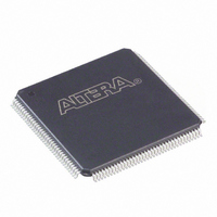
EP1C3T144C6N Altera, EP1C3T144C6N Datasheet - Page 27

EP1C3T144C6N
Manufacturer Part Number
EP1C3T144C6N
Description
IC CYCLONE FPGA 2910 LE 144-TQFP
Manufacturer
Altera
Series
Cyclone®r
Datasheet
1.EP1C3T144C8.pdf
(106 pages)
Specifications of EP1C3T144C6N
Number Of Logic Elements/cells
2910
Number Of Labs/clbs
291
Total Ram Bits
59904
Number Of I /o
104
Voltage - Supply
1.425 V ~ 1.575 V
Mounting Type
Surface Mount
Operating Temperature
0°C ~ 85°C
Package / Case
144-TQFP, 144-VQFP
Family Name
Cyclone®
Number Of Logic Blocks/elements
2910
# I/os (max)
104
Frequency (max)
405.2MHz
Process Technology
0.13um (CMOS)
Operating Supply Voltage (typ)
1.5V
Logic Cells
2910
Ram Bits
59904
Operating Supply Voltage (min)
1.425V
Operating Supply Voltage (max)
1.575V
Operating Temp Range
0C to 85C
Operating Temperature Classification
Commercial
Mounting
Surface Mount
Pin Count
144
Package Type
TQFP
Lead Free Status / RoHS Status
Lead free / RoHS Compliant
Number Of Gates
-
Lead Free Status / Rohs Status
Compliant
Other names
544-1662
Available stocks
Company
Part Number
Manufacturer
Quantity
Price
Company:
Part Number:
EP1C3T144C6N
Manufacturer:
ALTERA
Quantity:
250
Part Number:
EP1C3T144C6N
Manufacturer:
ALTERA
Quantity:
20 000
Figure 2–14. Shift Register Memory Configuration
Altera Corporation
May 2008
w
w
w
w
w × m × n Shift Register
m-Bit Shift Register
m-Bit Shift Register
m-Bit Shift Register
m-Bit Shift Register
register outputs (number of taps n × width w) must be less than the
maximum data width of the M4K RAM block (×36). To create larger shift
registers, multiple memory blocks are cascaded together.
Data is written into each address location at the falling edge of the clock
and read from the address at the rising edge of the clock. The shift register
mode logic automatically controls the positive and negative edge
clocking to shift the data in one clock cycle.
memory block in the shift register mode.
Memory Configuration Sizes
The memory address depths and output widths can be configured as
4,096 × 1, 2,048 × 2, 1,024 × 4, 512 × 8 (or 512 × 9 bits), 256 × 16 (or 256 × 18
bits), and 128 × 32 (or 128 × 36 bits). The 128 × 32- or 36-bit configuration
Figure 2–14
w
w
w
w
Embedded Memory
shows the M4K
n Number
of Taps
Preliminary
2–21


