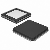
XC95288XL-7PQG208I Xilinx Inc, XC95288XL-7PQG208I Datasheet

XC95288XL-7PQG208I
Specifications of XC95288XL-7PQG208I
Available stocks
Related parts for XC95288XL-7PQG208I
XC95288XL-7PQG208I Summary of contents
Page 1
... C to +70° Description The XC95288XL is a 3.3V CPLD targeted for high-perfor- mance, low-voltage applications in leading-edge communi- © 1998-2007 Xilinx, Inc. All rights reserved. All Xilinx trademarks, registered trademarks, patents, and disclaimers are as listed at http://www.xilinx.com/legal.htm. All other trademarks and registered trademarks are the property of their respective owners. All specifications are subject to change without notice. ...
Page 2
... XAPP114, “Understanding XC9500XL CPLD Power.” 550 500 450 400 350 300 250 94 MHz 200 150 100 50 0 100 50 Clock Frequency (MHz) Figure 1: Typical I vs. Frequency for XC95288XL CC 2 208 MHz 200 250 150 DS055_01_121501 www.xilinx.com 1-800-255-7778 R DS055 (v2.1 April 3, 2007 Product Specification ...
Page 3
... I/O/GTS Function Block outputs (indicated by the bold line) drive the I/O Blocks directly. DS055 (v2.1 April 3, 2007 Product Specification JTAG In-System Programming Controller Controller I/O Blocks Figure 2: XC95288XL Architecture www.xilinx.com 1-800-255-7778 XC95288XL High Performance CPLD 54 Function 18 Block 1 Macrocells Function 18 Block 2 Macrocells ...
Page 4
... XC95288XL High Performance CPLD Absolute Maximum Ratings Symbol V Supply voltage relative to GND CC V Input voltage relative to GND IN V Voltage applied to 3-state output TS T Storage temperature (ambient) STG T Junction temperature J Notes: 1. Maximum DC undershoot below GND must be limited to either 0. mA, whichever is easier to achieve. During transitions, the device pins may undershoot to – ...
Page 5
... Output Type V CCIO 3.3V 2. Figure 3: AC Load Circuit www.xilinx.com 1-800-255-7778 XC95288XL High Performance CPLD XC95288XL-7 XC95288XL-10 Min Max Min Max - 7.5 - 10.0 4 4.5 - 5.8 - 125.0 - 100.0 1.6 - 2 ...
Page 6
... XC95288XL High Performance CPLD Internal Timing Parameters Symbol Parameter Buffer Delays T Input buffer delay IN T GCK buffer delay GCK T GSR buffer delay GSR T GTS buffer delay GTS T Output buffer delay OUT T Output buffer enable/disable EN delay Product Term Control Delays T Product term clock delay ...
Page 7
... H4 J2 768 765 4 15 – – 762 759 4 17 – – 756 4 18 www.xilinx.com 1-800-255-7778 XC95288XL High Performance CPLD TQ144 PQ208 BG256 FG256 CS280 – – – – – – – – – – – – – – – ...
Page 8
... XC95288XL High Performance CPLD XC95288XL I/O Pins (Continued) Func- tion Macro Block cell TQ144 PQ208 BG256 FG256 CS280 5 1 – – – – – – – – – – – (1) (1) ( – – – – – – – – – – ...
Page 9
... E10 A10 327 12 17 – – 324 12 18 www.xilinx.com 1-800-255-7778 XC95288XL High Performance CPLD TQ144 PQ208 BG256 FG256 CS280 – – – – – – 87 Y15 P10 W13 60 88 V14 T12 V13 – – – ...
Page 10
... XC95288XL High Performance CPLD XC95288XL I/O Pins (Continued) Func- tion Macro Block cell TQ144 PQ208 BG256 FG256 CS280 13 1 – – – 103 Y20 13 3 – 106 V19 13 4 – – – – 107 U19 13 6 – 109 T17 13 7 – ...
Page 11
... R XC95288XL Global, JTAG and Power Pins Pin Type TQ144 I/O/GCK1 30 I/O/GCK2 32 I/O/GCK3 38 I/O/GTS1 5 I/O/GTS2 6 I/O/GTS3 2 I/O/GTS4 3 I/O/GSR 143 TCK 67 TDI 63 TDO 122 TMS 65 V 3.3V 8, 42, 84, 141 CCINT V 2.5V/3 37, 55, 73, 109, CCIO 127 GND 18, 29, 36, 47, 62, 72, 89, 90, 99, 108, 114, 123, ...
Page 12
... XC95288XL High Performance CPLD Device Part Marking and Ordering Combination Information Device Type Package Speed Operating Range Speed Device Ordering and (pin-to-pin Part Marking Number delay) XC95288XL-6TQ144C 6 ns XC95288XL-6PQ208C 6 ns XC95288XL-6BG256C 6 ns XC95288XL-6FG256C 6 ns XC95288XL-6CS280C 6 ns XC95288XL-7TQ144C 7.5 ns XC95288XL-7PQ208C 7.5 ns XC95288XL-7BG256C 7 ...
Page 13
... XC95288XL-6PQG208C 6 ns XC95288XL-6BGG256C 6 ns XC95288XL-6FGG256C 6 ns XC95288XL-6CSG280C 6 ns XC95288XL-7TQG144C 7.5 ns XC95288XL-7PQG208C 7.5 ns XC95288XL-7BGG256C 7.5 ns XC95288XL-7FGG256C 7.5 ns XC95288XL-7CSG280C 7.5 ns XC95288XL-7TQG144I 7.5 ns XC95288XL-7PQG208I 7.5 ns XC95288XL-7BGG256I 7.5 ns XC95288XL-7FGG256I 7.5 ns XC95288XL-7CSG280I 7.5 ns XC95288XL-10TQG144C 10 ns XC95288XL-10PQG208C 10 ns XC95288XL-10BGG256C 10 ns XC95288XL-10FGG256C 10 ns XC95288XL-10CSG280C 10 ns XC95288XL-10TQG144I 10 ns XC95288XL-10PQG208I ...
Page 14
... XC95288XL High Performance CPLD Warranty Disclaimer THESE PRODUCTS ARE SUBJECT TO THE TERMS OF THE XILINX LIMITED WARRANTY WHICH CAN BE VIEWED AT http://www.xilinx.com/warranty.htm. THIS LIMITED WARRANTY DOES NOT EXTEND TO ANY USE OF THE PRODUCTS IN AN APPLICATION OR ENVIRONMENT THAT IS NOT WITHIN THE SPECIFICATIONS STATED ON THE THEN-CURRENT XILINX DATA SHEET FOR THE PRODUCTS ...


