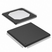
XC95288XL-10TQ144I Xilinx Inc, XC95288XL-10TQ144I Datasheet - Page 4

XC95288XL-10TQ144I
Manufacturer Part Number
XC95288XL-10TQ144I
Description
HP CPLD TQ FLAT 144 IND TMP P/P
Manufacturer
Xilinx Inc
Series
XC9500XLr
Datasheet
1.XC95288XL-10TQG144C.pdf
(14 pages)
Specifications of XC95288XL-10TQ144I
Programmable Type
In System Programmable (min 10K program/erase cycles)
Delay Time Tpd(1) Max
10.0ns
Voltage Supply - Internal
3 V ~ 3.6 V
Number Of Logic Elements/blocks
16
Number Of Macrocells
288
Number Of Gates
6400
Number Of I /o
117
Operating Temperature
-40°C ~ 85°C
Mounting Type
Surface Mount
Package / Case
144-TQFP, 144-VQFP
Voltage
3.3V
Memory Type
FLASH
Lead Free Status / RoHS Status
Contains lead / RoHS non-compliant
Features
-
Number Of Logic Elements/cells
-
Other names
155632
Q1155632
XC95288XL10TQ144I
Q1155632
XC95288XL10TQ144I
Available stocks
Company
Part Number
Manufacturer
Quantity
Price
Company:
Part Number:
XC95288XL-10TQ144I
Manufacturer:
JST
Quantity:
12 000
Part Number:
XC95288XL-10TQ144I
Manufacturer:
XILINX/赛灵思
Quantity:
20 000
XC95288XL High Performance CPLD
Absolute Maximum Ratings
Recommended Operation Conditions
Quality and Reliability Characteristics
DC Characteristic Over Recommended Operating Conditions
4
Notes:
1.
2.
3.
Symbol
Symbol
Maximum DC undershoot below GND must be limited to either 0.5V or 10 mA, whichever is easier to achieve. During transitions, the
device pins may undershoot to –2.0V or overshoot to +7.0V, provided this over- or undershoot lasts less than 10 ns and with the
forcing current being limited to 200 mA. External I/O voltage may not exceed V
Stresses beyond those listed under Absolute Maximum Ratings may cause permanent damage to the device. These are stress
ratings only, and functional operation of the device at these or any other conditions beyond those listed under Operating Conditions
is not implied. Exposure to Absolute Maximum Ratings conditions for extended periods of time may affect device reliability.
For soldering guidelines and thermal considerations, see the
packages, see XAPP427.
V
Symbol
Symbol
V
C
I
V
I
I
I
CC
V
V
OH
IH
IH
T
OL
IL
T
N
IN
V
CCINT
V
V
V
CCIO
V
V
ESD
STG
T
DR
PE
CC
TS
IN
IH
IL
O
J
Output high voltage for 3.3V outputs
Output high voltage for 2.5V outputs
Output low voltage for 3.3V outputs
Output low voltage for 2.5V outputs
Input leakage current
I/O high-Z leakage current
I/O high-Z leakage current
I/O capacitance
Operating supply current
(low power mode, active)
Data Retention
Program/Erase Cycles (Endurance)
Electrostatic Discharge (ESD)
Supply voltage relative to GND
Input voltage relative to GND
Voltage applied to 3-state output
Storage temperature (ambient)
Junction temperature
Supply voltage for internal logic
and input buffers
Supply voltage for output drivers for 3.3V operation
Supply voltage for output drivers for 2.5V operation
Low-level input voltage
High-level input voltage
Output voltage
Parameter
Parameter
(2)
Description
Parameter
(1)
(3)
(1)
www.xilinx.com
1-800-255-7778
I
I
I
I
V
V
V
V
V
V
V
Commercial T
Industrial T
OH
OH
OL
OL
CC
CC
CC
IN
CC
IN
IN
= 8.0 mA
= 500 μA
= –500 μA
= –4.0 mA
= GND or 3.6V
= GND; f = 1.0 MHz
= GND, No load; f = 1.0 MHz
= Max; V
= Max; V
= Max; V
Min < V
Device Packaging
Test Conditions
A
IN
= –40
IN
IN
CCIO
A
< 5.5V
= 0
= GND or V
= GND or V
o
= Max;
o
C to +85
C to 70
CCINT
information on the Xilinx website. For Pb-free
10,000
2,000
Min
20
by 4.0V.
o
CC
CC
C
o
C
–65 to +150
–0.5 to 4.0
–0.5 to 5.5
–0.5 to 5.5
Value
+150
Min
2.0
90% V
3.0
3.0
3.0
2.3
0
0
Max
Min
2.4
85 (Typical)
-
-
-
-
-
-
-
-
-
-
CCIO
DS055 (v2.1 April 3, 2007
V
Product Specification
Max
0.80
3.6
3.6
3.6
2.7
5.5
CCIO
Max
±10
±10
±10
±50
0.4
0.4
10
-
-
Units
Cycles
Years
Units
Volts
o
o
V
V
V
C
C
Units
Units
V
V
V
V
V
V
V
mA
μA
μA
μA
μA
pF
V
V
V
V
R


