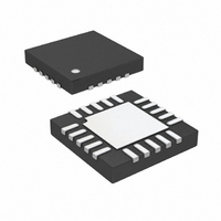
LTC2655IUF-H12#PBF Linear Technology, LTC2655IUF-H12#PBF Datasheet - Page 8

LTC2655IUF-H12#PBF
Manufacturer Part Number
LTC2655IUF-H12#PBF
Description
IC DAC 12BIT QUAD CUR OUT 20QFN
Manufacturer
Linear Technology
Datasheet
1.LTC2655CGN-H12PBF.pdf
(28 pages)
Specifications of LTC2655IUF-H12#PBF
Settling Time
3.9µs
Number Of Bits
12
Data Interface
I²C, Serial
Number Of Converters
4
Voltage Supply Source
Single Supply
Operating Temperature
-40°C ~ 85°C
Mounting Type
Surface Mount
Package / Case
20-WQFN Exposed Pad, 20-DQFN
Lead Free Status / RoHS Status
Lead free / RoHS Compliant
Power Dissipation (max)
-
Available stocks
Company
Part Number
Manufacturer
Quantity
Price
LTC2655
ELECTRICAL CHARACTERISTICS
LTC2655B-H16/LTC2655-H12 (Internal Reference = 2.048V)
SYMBOL
Reference
Power Supply
V
I
I
Digital I/O
V
V
V
V
V
V
R
R
R
V
t
t
I
C
C
C
8
temperature range, otherwise specifi cations are at T
CC
SD
OF
SP
IN
CC
IL
IH
IL(LDAC)
IH(LDAC)
IL(CA)
IH(CA)
OL
IN
B
CA n
INH
INL
INF
PARAMETER
Reference Output Voltage
Reference Temperature Coeffi cient
Reference Line Regulation
Reference Short-Circuit Current
REFCOMP Pin Short-Circuit Current
Reference Load Regulation
Reference Output Voltage Noise Density
Reference Input Range
Reference Input Current
Reference Input Capacitance
Positive Supply Voltage
Supply Current (Note 8)
Supply Current in Shutdown Mode (Note 8)
Low Level Input Voltage (SDA and SCL)
High Level Input Voltage (SDA and SCL)
Low Level Input Voltage (LDAC)
High Level Input Voltage (LDAC)
Low Level Input Voltage (CA0 to CA2)
High Level Input Voltage (CA0 to CA2)
Resistance from CAn ( n = 0,1,2)
to V
Resistance from CA n ( n = 0,1,2)
to GND to Set CA n = GND
Resistance from CA n ( n = 0,1,2)
to V
Low Level Output Voltage
Output Fall Time
Pulse Width of Spikes Suppressed by Input
Filter
Input Leakage
I/O Pin Capacitance
Capacitance Load for Each Bus Line
External Capacitive Load on Address Pins
CA0, CA1 and CA2
CC
CC
or GND to Set CA n = FLOAT
to Set CA n = V
CC
CONDITIONS
(Note 7)
V
V
V
V
C
External Reference Mode (Note 14)
(Note 9)
For Specifi ed Performance
V
V
V
V
V
See Test Circuit 1
See Test Circuit 1
See Test Circuit 2
See Test Circuit 2
See Test Circuit 2
Sink Current = 3mA
V
C
0.1V
(Note 9)
A
CC
CC
CC
CC
REFCOMP
CC
CC
CC
CC
CC
O
B
= 25°C. V
= 10pF to 400pF (Note 13)
= V
±10%
= 5.5V, Forcing REFIN/OUT to GND
= 5.5V, Forcing REFCOMP to GND
= 5V±10%, I
= 5V, Internal Reference On
= 5V, Internal Reference Off
= 5V
= 4.5V to 5.5V
= 4.5V to 5.5V
CC
IH(MIN)
≤ V
The
= C
IN
l
CC
≤ 0.9V
REFIN/OUT
to V
denotes the specifi cations which apply over the full operating
= 4.5V to 5.5V, V
OUT
O
= V
CC
= 100μA Sourcing
IL(MAX)
= 0.1μF , at f = 1kHz
,
OUT
unloaded unless otherwise specifi ed.
l
l
l
l
l
l
l
l
l
l
l
l
l
l
l
l
l
l
l
l
l
l
l
l
l
20+0.1C
0.85V
0.7V
2.044
MIN
0.5
4.5
2.4
2
0
0
CC
CC
B
2.048
0.001
TYP
–80
1.9
1.5
±2
65
40
35
20
3
0.15V
0.3V
V
2.052
MAX
±10
200
250
400
CC
5.5
2.5
0.8
0.4
10
10
50
10
10
5
1
2
3
1
/2
CC
CC
ppm/°C
mV/mA
nV/√Hz
UNITS
2655f
MΩ
mA
mA
mA
kΩ
kΩ
dB
μA
μA
μA
μA
pF
ns
ns
pF
pF
pF
V
V
V
V
V
V
V
V
V
V


