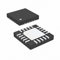
LTC2655IUF-H12#PBF Linear Technology, LTC2655IUF-H12#PBF Datasheet - Page 22

LTC2655IUF-H12#PBF
Manufacturer Part Number
LTC2655IUF-H12#PBF
Description
IC DAC 12BIT QUAD CUR OUT 20QFN
Manufacturer
Linear Technology
Datasheet
1.LTC2655CGN-H12PBF.pdf
(28 pages)
Specifications of LTC2655IUF-H12#PBF
Settling Time
3.9µs
Number Of Bits
12
Data Interface
I²C, Serial
Number Of Converters
4
Voltage Supply Source
Single Supply
Operating Temperature
-40°C ~ 85°C
Mounting Type
Surface Mount
Package / Case
20-WQFN Exposed Pad, 20-DQFN
Lead Free Status / RoHS Status
Lead free / RoHS Compliant
Power Dissipation (max)
-
Available stocks
Company
Part Number
Manufacturer
Quantity
Price
OPERATION
LTC2655
In this case, the power-up delay time is approximately
14μs. The power-up of the integrated reference depends
on the command that powered it down. If the reference is
powered down using the Select External Reference com-
mand (0111b), then it can only be powered back up by
sending the Select Internal Reference command (0110b).
However if the reference was powered down by sending
the Power-Down Chip command (0101b), then in addition
to the Select Internal Reference command (0110b), any
command that powers up the DACs will also power-up
the integrated reference.
Reference Modes
For applications where an accurate external reference is
not available, the LTC2655 has a user-selectable, inte-
grated reference. The LTC2655-L has a 1.25V reference
that provides a full-scale output of 2.5V. The LTC2655-H
has a 2.048V reference that provides a full-scale output
of 4.096V. Both references exhibit a typical temperature
drift of 2ppm/°C. Internal reference mode can be selected
by using command 0110b, and is the power-on default. A
buffer is needed if the internal reference is required to drive
external circuitry. For reference stability and low noise, it
is recommended that a 0.1μF capacitor be tied between
REFCOMP and GND. In this confi guration, the internal
reference can drive up to 0.1μF capacitive load without any
stability problems. In order to ensure stable operation, the
capacitive load on the REFIN/OUT pin should not exceed
the capacitive load on the REFCOMP pin.
The DAC can also operate in external reference mode using
command 0111b. In this mode, the REFIN/OUT pin acts
as an input that sets the DAC’s reference voltage. This
input is high impedance and does not load the external
reference source. The acceptable voltage range at this
pin is 0.5V ≤ REFIN/OUT ≤ V
output voltage is 2•V
ence at start-up, see the Power Supply Sequencing and
Start-Up Sections.
22
REFIN/OUT
CC
/2. The resulting full-scale
. For using external refer-
Integrated Reference Buffers
Each of the four DACs in LTC2655 has its own integrated
high performance reference buffer. The buffers have very
high input impedance and do not load the reference volt-
age source. These buffers shield the reference voltage
from glitches caused by DAC switching and thus minimize
DAC-to-DAC dynamic crosstalk. By tying 0.22μF capacitors
between REFCOMP and GND, and also between REFIN/OUT
See the curve DAC-to-DAC Crosstalk (Dynamic) in the
Typical Performance Characteristics section.
Voltage Outputs
Each of the four rail-to-rail amplifi ers contained in LTC2655
has guaranteed load regulation when sourcing or sinking
up to 15mA at 5V (7.5mA at 3V).
Load regulation is a measure of the amplifi er’s ability to
maintain the rated voltage accuracy over a wide range of
load conditions. The measured change in output voltage
per milliampere of forced load current change is expressed
in LSB/mA.
DC output impedance is equivalent to load regulation, and
may be derived from it by simply calculating a change in
units from LSB/mA to ohms. The amplifi ers’ DC output
impedance is 0.040Ω when driving a load well away from
the rails.
When drawing a load current from either rail, the output
voltage headroom with respect to that rail is limited by
the 30Ω typical channel resistance of the output devices;
e.g., when sinking 1mA, the minimum output voltage =
30Ω • 1mA = 30mV. See the graph Headroom at Rails vs
Output Current in the Typical Performance Characteristics
section.
The amplifi ers are stable driving capacitive loads of up
to 1000pF .
and GND, the crosstalk can be reduced to less than 1nV•s.
2655f


