MAX5891EGK+D Maxim Integrated Products, MAX5891EGK+D Datasheet - Page 10
MAX5891EGK+D
Manufacturer Part Number
MAX5891EGK+D
Description
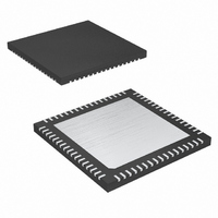
IC DAC 16BIT LVDS 600MSPS 68-QFN
Manufacturer
Maxim Integrated Products
Datasheet
1.MAX5891EGKD.pdf
(16 pages)
Specifications of MAX5891EGK+D
Settling Time
11ns
Number Of Bits
16
Data Interface
Parallel
Number Of Converters
1
Voltage Supply Source
Analog and Digital
Power Dissipation (max)
301mW
Operating Temperature
-40°C ~ 85°C
Mounting Type
Surface Mount
Package / Case
68-QFN Exposed Pad
Conversion Rate
600 MSPs
Resolution
16 bit
Interface Type
Parallel or LVDS
Supply Voltage (max)
1.89 V, 3.465 V
Supply Voltage (min)
1.71 V, 3.135 V
Maximum Operating Temperature
+ 85 C
Mounting Style
SMD/SMT
Minimum Operating Temperature
- 40 C
Lead Free Status / RoHS Status
Lead free / RoHS Compliant


To achieve the best possible jitter performance, the
MAX5891 features flexible differential clock inputs
(CLKP, CLKN) that operate from a separate clock
power supply (AV
inputs from a single-ended or a differential clock
source. For highest dynamic performance, differential
clock source is required. For single-ended operation,
drive CLKP and bypass CLKN to CGND.
CLKP and CLKN are internally biased at AV
allowing the AC-coupling of clock sources directly to
the device without external resistors to define the DC
level. The input resistance from CLKP and CLKN to
ground is approximately 5kΩ.
16-Bit, 600Msps, High-Dynamic-Performance
DAC with LVDS Inputs
Figure 2. Simplified Analog Output Structure
Figure 3. Timing Relationship Between Clock, Input Data, and Analog Output
10
AV
SWITCHES
D0–D16
CURRENT
IOUTN
IOUTP
DD3.3
CLKP
CLKN
______________________________________________________________________________________
t
SETUP
CURRENT
SOURCES
OUT
CLK
Clock Inputs (CLKP, CLKN)
D
N - 7
N
). Drive the differential clock
OUT
N - 6
D
N + 1
I
OUT
OUTN OUTP
t
HOLD
OUT
D
N - 5
N + 2
CLK
I
OUT
/ 2,
OUT
N - 4
D
N + 3
Figure 3 shows the timing relationship between digital
LVDS data, clock, and output signals. The MAX5891
features a 2.6ns hold, a -1.5ns setup, and a 2.5ns prop-
agation delay time. There is a 5.5 clock-cycle latency
between data write operation and the corresponding
analog output transition.
The MAX5891 has 16 pairs of LVDS data inputs (offset
binary format) and can accept data rates up to
600Mwps. Each differential input pair is terminated with
an internal 110Ω resistor. The common-mode input
resistance is 3.2kΩ.
The MAX5891 features a power-down mode that
reduces the DAC’s power consumption. Set PD high to
power down the MAX5891. Set PD low or leave uncon-
nected for normal operation.
When powered down, the MAX5891 overall power con-
sumption is reduced to less than 13µW. The MAX5891
requires 350µs to wake up from power-down and enter
a fully operational state if the external reference is
used. If the internal reference is used, the power-down
recovery time is 10ms. The PD internal pulldown circuit
sets the MAX5891 in normal mode when PD is left
unconnected.
OUT
N - 3
D
N + 4
t
PD
OUT
D
N + 5
N - 2
Power-Down Operation (PD)
Data-Timing Relationship
OUT
N-1
D
N + 6
LVDS Data Inputs
OUT
N
D
N + 7
Related parts for MAX5891EGK+D
Image
Part Number
Description
Manufacturer
Datasheet
Request
R

Part Number:
Description:
16-Bit/ 600Msps -High-Dynamic-Performance/DAC with LVDS Inputs
Manufacturer:
Maxim Integrated Products
Datasheet:

Part Number:
Description:
Max5891 16-bit, 600msps, High-dynamic-performance Dac With Lvds Inputs
Manufacturer:
Maxim Integrated Products, Inc.
Datasheet:
Part Number:
Description:
MAX7528KCWPMaxim Integrated Products [CMOS Dual 8-Bit Buffered Multiplying DACs]
Manufacturer:
Maxim Integrated Products
Datasheet:
Part Number:
Description:
Single +5V, fully integrated, 1.25Gbps laser diode driver.
Manufacturer:
Maxim Integrated Products
Datasheet:
Part Number:
Description:
Single +5V, fully integrated, 155Mbps laser diode driver.
Manufacturer:
Maxim Integrated Products
Datasheet:
Part Number:
Description:
VRD11/VRD10, K8 Rev F 2/3/4-Phase PWM Controllers with Integrated Dual MOSFET Drivers
Manufacturer:
Maxim Integrated Products
Datasheet:
Part Number:
Description:
Highly Integrated Level 2 SMBus Battery Chargers
Manufacturer:
Maxim Integrated Products
Datasheet:
Part Number:
Description:
Current Monitor and Accumulator with Integrated Sense Resistor; ; Temperature Range: -40°C to +85°C
Manufacturer:
Maxim Integrated Products
Part Number:
Description:
TSSOP 14/A°/RS-485 Transceivers with Integrated 100O/120O Termination Resis
Manufacturer:
Maxim Integrated Products
Part Number:
Description:
TSSOP 14/A°/RS-485 Transceivers with Integrated 100O/120O Termination Resis
Manufacturer:
Maxim Integrated Products
Part Number:
Description:
QFN 16/A°/AC-DC and DC-DC Peak-Current-Mode Converters with Integrated Step
Manufacturer:
Maxim Integrated Products
Part Number:
Description:
TDFN/A/65V, 1A, 600KHZ, SYNCHRONOUS STEP-DOWN REGULATOR WITH INTEGRATED SWI
Manufacturer:
Maxim Integrated Products
Part Number:
Description:
Integrated Temperature Controller f
Manufacturer:
Maxim Integrated Products
Part Number:
Description:
SOT23-6/I°/45MHz to 650MHz, Integrated IF VCOs with Differential Output
Manufacturer:
Maxim Integrated Products
Part Number:
Description:
SOT23-6/I°/45MHz to 650MHz, Integrated IF VCOs with Differential Output
Manufacturer:
Maxim Integrated Products